Thursday, July 30, 2009

Grafik Untuk Menentukan Ukuran Box|Kotak Speaker

The problems that often appear when you want to make a speaker box set itself is large so that the required optimal results? When the box is too large, then the low tones produced less power, but if it feels too small voices will explode feel-ledak low frequency response and the resulting reduced. In short, either too large or too small so low a tone you would expect we will not be generated properly. Akan problems but most of the other speakers in the local market does not have nearly the complete list with the specification. Usually only the size of the diameter, Impedance nominal and maximum power, such as 12 ", 8 Ohm, 400 watts. That's it.

Based on a book publication that includes techniques to create speaker closed with a conventional way using only standard diameter speaker. In the book charts given volume needed by the speaker based on the diameter of a closed box speakers are as follows:

Ukuran Box SpeakerGrafik Untuk Menentukan Ukuran Box|Kotak Speaker

With:
X = Diameter speaker
Y = volume Box (in Litre)
Diameter SpeakerDiameter Speaker

The graph above shows the limit above and below the limit of the required volume in liters. For example, the speaker berdiameter 6 "- 6.5" that many circulating in the market, the volume required is between 8.8 liters to 12.7 liters. The graph is expected to be useful for many who want to make a good speaker system using the materials in the local market

and the following list of Size Speaker Box based manufacturer ACR output, you can also use it
  • 12″ ACR – 12360 – 139.53 liter
  • 12″ ACR – 12380 – 124 liter
  • 12″ ACR – 1225 – 173.19 liter
  • 12″ ACR – 1240 – 79 liter
  • 10″ PA – 10880 – 42 liter
  • 12″ PA – 12880 – 103 liter
  • 15″ ACR 15610 – 222 liter
  • 15″ ACR 15750 – 155.62 liter
  • 15″ ACR DELTA 15 – 188 liter
  • 18″ AX 18420 GRAND ACR NEW 450 liter
  • 21″ AX 21800 GRAND ACR NEW 640 liter
Note:
  • A litre is defined as a special name for a cubic decimetre (1 L = 1 dm^3 = 1000 cm^3). Hence 1 L ≡ 0.001 m^3 (exactly). So 1000 L = 1 m^3 (see table below)
table liter to cm3Table litre to cm3

Source www.banuaji.blogspot.com

Wednesday, July 29, 2009

RANGKAIAN DOWNLOADER AVR MIKROKONTROLLER

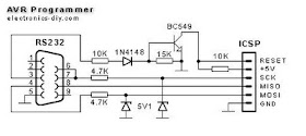
This is a simple circuit of downloader AVR microcontrollers (Atmega|Attiny ). This circuit can be used to painlessly transfer hex programs to most ATMEL AVR microcontrollers without sacrificing your budget and time. It is more reliable than most other simple AVR downloader programmers available out there and can be built in very short amount of time.

AVR downloader programmer consists of in-circuit serial programmer (dongle) and small pcb with a DIP socket where you can fit your microcontroller and have it quickly downloader programmed.

Entire AVR downloader programmer has been build with using common parts and fits in the case of the serial connector. The socket pcb has been created to fit a 28-DIP AVR ATmega8 microcontroller, but you can build a socket pcb for any other AVR microcontroller out there. This AVR programmer is compatible with a popular PonyProg software that shows you a status bar of the programming progress.
AVR Downloader Mikrokontrolleravr (Atmega|Attiny) Downloader Mikrokontroller

AVR Downloader MikrokontrollerSkema rangkaian Downloader AVR (Atmega|Attiny) mikrokontroller

AVR Downloader MikrokontrollerAVR Downloader Mikrokontroller
Finished AVR (ATmega|Attiny) Downloader Programmer with standard 6-PIN ICSP connector.


Make AVR Socket PCB

Socket PCB consists of the PCB, 28-DIP socket, 4MHz crystal resonator, or crystal with two 22pF decoupling capacitors, and two header connectors. Two-PIN connector supplies +5V voltage to the AVR microcontroller, and 6-PIN ICSP connects to AVR Programmer dongle.

Supplying microcontroller with external +5V voltage as opposed to taking it directly from computer's serial connection port ensures that the chip is receiving exactly +5V voltage and provides very reliable error free programming. +5V voltage supply for AVR mikrokontroller chip may be provided from external power supply or even better - directly from USB connection.
AVR Downloader Mikrokontroller

AVR Downloader MikrokontrollerFinished Socket PCB AVR ATmega8 microcontroller pic

Rangkaian Low pass Filter aktif

frequencies higher than the cutoff frequency. The actual amount of attenuation for each frequency varies from filter to filter. It is sometimes called a high-cut filter, or treble cut filter when used in audio applications. A low-pass filter is the opposite of a high-pass filter, and a band-pass filter is a combination of a low-pass and a high-pass.

The concept of a low-pass filter exists in many different forms, including electronic circuits (like a hiss filter used in audio), digital algorithms for smoothing sets of data, acoustic barriers, blurring of images, and so on.

in the image below in the show Rangkaian Aktif low pass filter using op amp lm 741:

Skema rangkaian Active Lowpass FilterSkema rangkaian Low pass Filter aktif

In the operational amplifier circuit shown in the figure, the cutoff frequency (in hertz) is defined as:
Rumus Active Lowpass Filter

or equivalently (in radians per second):
Rumus Active Lowpass Filter

The gain in the passband is
\frac{-R_2}{R_1}

and the stopband drops off at −6 dB per octave as it is a first-order filter.


Sometimes, a simple gain amplifier (as opposed to the very-high-gain operation amplifier) is turned into a low-pass filter by simply adding a feedback capacitor C. This feedback decreases the frequency response at high frequencies via the Miller effect, and helps to avoid oscillation in the amplifier. For example, an audio amplifier can be made into a low-pass filter with cutoff frequency 100 kHz to reduce gain at frequencies which would otherwise oscillate. Since the audio band (what we can hear) only goes up to 20 kHz or so, the frequencies of interest fall entirely in the passband, and the amplifier behaves the same way as far as audio is concerned.


Tuesday, July 28, 2009

Rangkaian Subwoofer 200 watt

If we walk in the shop or mall and see the electronic equipment is high end, so sometimes we desire to have the equipment, for example, we see that a subwoofer bass sound is so excite. but for the price of our audio equipment may still include expensive

As an electrician we have any idea, how to make a quality subwoofer, such as not lose it in the store, but with an affordable cost.

Music of heave fluty, plus the subwoofer with the boom of the formations, it is that we want to show in this project. a series of simple and inexpensive numun able to meet the conditions above.
Skema Rangkaian Subwoofer Skema rangkaian Subwoofer

Active Subwoofer (rangkaian subwoofer) is a series of Simple and simple before trying this series to prepare yourself to listen to the crack formations that will be generated by this series. power amplifier for its series, please use the power that you like our previous post. However, to use the results of the maximal power with a higher power. for example, using the power that has STK4050 power 200 watt.

To suuplay series of the above you can use the IC regulator 7815 and 7915 or more can be seen here


Skema 200 watt Power Amplifier STK4050 II

Features STK4050 II
  • Compact package for thin-type audio sets
  • Member of pin-compatible series with outputs of 20 to
  • 200W
  • Easy heatsink design to disperse heat generated in thintype
  • stereo sets
  • Constant-current circuit to reduce supply switch-on and
  • switch-off shock noise
  • External supply switch-on and switch-off shock noise
  • muting, load short-circuit protection, thermal shutdown
  • and other circuits can be tailored-designed

Application Circuit Power Amplifier STK4050 II

Skema Power Amplifier STK4050 IISkema Specified Transformer Supply for 200 watt Power Amplifier STK4050 II

Supplay 200 watt Power Amplifier
Note:
  • To use the results of the max capacitor 10000Uf/80 Vot, with a pure tranformator 5 / 42 volt
  • provide a good cooling plate, the ic STK4050 II


Tips that sub Woofer Voice | bass sound more felt

according to experience, you have to do a little experiment for you to get the best bass sound, stalwart, gigantic. To get the best bass sound between the subwoofer and the room you, then you should get a 'pass that point. the following manner:
  • Place the subwoofer on your location on our seat. (sub Woofer do not be put on the table / cupboard you high more than 1 / 2 meter)
  • Turn the sub Woofer and you do not forget to disconnect the speaker Amplifier.
  • Play a song you like, which have gained a good frequency bass
  • Then try running memutari room, see the characters that appear bass.
  • You will hear some of the bass sound quality improvements in some corner of the room. This happens due to the interaction between low-frequency space and you. Nah corners you can select as a "node" or the point pas you need to immediately place your subwoofer in a corner of it.

Pengertian Daya dalam watt PMPO dan RMS

Compo sound device or active speaker with built-in speaker PMPO with generally stated, a value that is usually put in the large 500 watt PMPO, 1000 watt PMPO, or even more.

PMPO (peak music power output) and currents measured by the peak voltage that can be issued an amplifier. Unit size of PMPO power is not a standard. This size refers to the highest point of the sound that comes from a series of spiker. Value and each spiker and then combined, and reproducible. For example, with five surround spiker with power spiker each 10 Watt, the ability spiker is 100 Watts PMPO.

However, for practitioners engaged in the field of audio, this count does not become a criterion when choosing spiker. Counts RMS (Root Mean Square) is a trusted reference. This calculation will determine the average power output from a sound system spiker. This value is usually listed on the carton or product information with the extension "Watts RMS." The greater the value, meaning the output of the more forceful voice spiker.

Options RMS value also depends on taste. If you like the sound spiker bass rumble, then choose the spiker the RMS value to its high


Monday, July 27, 2009

Rangkaian Konfigurasi Common Emitter dan Collector

Rangkain Konfigurasi Common Emitte

Transistor configuration that is most often found configuration Common Emitter (CE). Called the Common Emitter (CE) as the emitter on the side with the input and output.
Konfigurasi Common EmitteRangkain Konfigurasi Common Emitte

In this configuration, the relationship between the flow base, emitter and collector is fixed.
  • IE = IB + IC
In the configuration Emitter Common characteristics of the output is kurva between the output currents to the IC output voltage VCE at a flow rate range of input IB. Characteristics kurva input is the input current IB to the input voltage VBE on the value of output voltage VCE.
Rangkain Konfigurasi Common EmitteKurva Karakteritik Output & Kurva Karakteritik Input

Note that the output characteristics kurva, IB current does not horizontally as well as IE in common base configuration, the indicates that the collector-voltage emiter (VCE) affect the amount of current collector. Active area for common emitter configuration is a region in the top right where IB kurva flow near straight line (linear). In the picture, this region is located on the right-VCE sat and above kurva IB = 0. Area in the left-VCE sat is the saturation. Flow conditions on the collector IB = 0 is expressed as follows:

In DC mode, IB and IC level associated with a defined amount of beta:


In the specification / data sheet, βdc written hFE. To ac mode:


Ac strengthening also known as hfe. (note the difference with hFE) Βdc and βac generally worth the same as written and β only. The relationship between β and α are as follows:


With IC = βIB can also be derived:


Rangkaian Konfigurasi Common Collector

Common Collector configuration is generally used as a series of adjustments because Impedance Impedance has a high input and low output Impedance, contrary to the two previous configurations (CB and CE).
Characteristics of CC input configuration is the same as the characteristics of the CE configuration. Output characteristics is a plot of IE with the VEC for the values of IB, kurva form with the same characteristics as the output CE.
Rangkaian Konfigurasi Common Collector Rangkaian Konfigurasi Common Collector

Sunday, July 26, 2009

Rangkaian Common Base Configuration

Transistors operating

Transistor operating with a bias in both Junction (base-emitter and base-collector). Total current from the emitter terminal is the same as the flow in the collector terminal on the terminal plus cash basis.
  • IE = IB + IC
ICO value is very small and generally can be ignored Base-emitter voltage (VBE) can be considered as a variable in determining the controller transistor operation

Collector current IC of the proportional relationship with the current IB IC = β IB. The greater the flow of IB also IC flow, seems to have the flow. Data specification transistor (from factory) in the set maximum value that should not be dilampaui in operation. This specification provides limits of transistor operation in the series.

Collector current IC consists of two components, originating from the majority carrier and minority carrier. Flow of minority carriers is called the ICO
  • IC = IC majority + ICO minority
ICO value is very small and generally can be ignored Base-emitter voltage (VBE) can be considered as a variable in determining the controller transistor operation

Collector current IC of the proportional relationship with the current IB IC = β IB. The greater the current of IB also current IC. Data specification transistor (from factory) in the set maximum value that should not be skipped in the operation. This specification provides limits of transistor operation in the series.


Common Base Configuration

Naming base comes from the common condition where the base used in the joint input and output.

Rangkain Common Base Configuration

Direction of flow indicated is the direction of conventional flow. Characteristics such as the strengthening of this characteristic is described in kurva input and output characteristics kurva. Characteristics between the input current IE to the input voltage VBE for some value of output voltage VCB. Characteristics of the output current output voltage of IC output for some values VCB IE.

Rangkain Common Base Configuration
Kurva Karakteristik input & output Common Base Configuration

Characteristics of output has three working areas, namely active, the cut-off and saturation. Active region is a region where the linear case. Specifically stated: "In the active region, Junction base-collector reverse bias while at the Junction in the base-emitter forward bias. "

At the bottom of the active region, where the emitter current IE = 0, collector currents flow only from behind the ICO the saturation value is very small (in the micro-ampere), so it can be ignored.

the cut-off is defined as the area where the current IC = 0 A. or indicate : "Regional cut-off occurs when Junction base-collector and base-emitter Junction in reverse bias."

Saturation region is a region where the value of a negative voltage VCB. or indicate: "Region is a region where saturation Junction base-collector and base-emitter Junction in forward bias."

Characteristics of the input seen that for fixed value of VCB, when the base-emitter voltage (VBE) has increased, flow increased as well as the emitter on the diode. Raising the voltage VCB has a very small impact so that it can be ignored. Model ekivalen input from kurva characteristics are as following picture:

Rangkain Common Base Configuration
In further analysis, when the transistor is in a condition "on", the assumed base-emitter voltage:

Alpha
In DC mode, flow-level IC and IE comes from the majority carriers have a relationship:

Because α is determined from the majority carrier, then


ICBO generally very small so it can be ignored. For ac current, α is defined:

αac formally known as the common base, chort circuit, amplification factor. Value αac and αdc quite close, so often expressed as α only.

Rangkaian Antarmuka Seven Segmen Dengan AT89S51/52

Data that is processed mikrokontroler data hexa, to be shown on seven segment we can use dekoder hexa to the sevent segment or through the conversion program, for konveri, we can use the system look up table program we need a conversion table, table is as follows:

Place the module with mikrokontroler seven segment connecting module on port 1 and 3, do not look up inverted. Seven segment that is in use CA (Common Anode), thus need to be given to set the logic 0.
Antarmuka Seven Segmen-AT89S51/52Scheme of the Seven-segment

Antarmuka Seven Segmen-AT89S51/52The Switch scheme Electronics

Antarmuka Seven Segmen-AT89S51/52
;=================================================
;PROGRAM To turn 4X 7SEGMENT COMMON ANODA
;=================================================
ORG 00H
MULAI:
MOV P1,#0C7H ;display, data 0
CLR P3.4 ;Turn on COMMON 1
CALL DELAY ;Delay
SETB P3.4 ; turn off COMMON 1
CALL DELAY ;Delay
MOV P1,#040H ;display, data 1
CLR P3.5
CALL DELAY
SETB P3.5
CALL DELAY
MOV P1,#042H ;display, data 2
CLR P3.6
CALL DELAY
SETB P3.6
CALL DELAY
MOV P1,#050H ;display, data 3
CLR P3.7
CALL DELAY
SETB P3.7
CALL DELAY
AJMP MULAI
DELAY: ;Pause THIS USED 7SEGMENT To be invisibl
MOV R1,#1
DELAY1: DJNZ R0,$
DJNZ R1,DELAY1
RET
END

Rangkaian Saklar|Keypad Matrix AT89S51/52

Rangkaian saklar for mikrokontroler AT89S51/52

Port mikrokontroler AT89S51/52 The complete internal pull-up, a default condition so that it is high. To make this port as input, we live to provide logic high or ignore in the default condition. If we want a legible entries we should use the Low input signal.

In the picture below, when the button on the keypad and press the low signal will be sent to port 3 on mikrokontroler, Thus, this port will have a logic in accordance with the key emphasis

saklar|Keypad MatrikSkema Rangkaia Mikrokontroler dengan masukan Saklar

;---------------------------------------------------------------------
; Simulasi penekanan tombol pd P3.0 untuk menghidupkan
; dan P3.1 untuk mematikan LED pada Port 1
;----------------------------------------------------------------------
ORG 0H
MULAI:
MOV A,P3 ; Baca port 3
CJNE A,#0FEH,TERUS ; Apakah isi akumulator = 11111110B
MOV P1,#000H ; Ya! Hidupkan lampu LED di port 1
SJMP MULAI ; Ulangi lagi dari awal
TERUS:
CJNE A,#0FDH,MULAI ; Apakah isi akumulator = 11111101B
MOV P1,#0FFH ; Ya! Matikan lampu LED di port 1
SJMP MULAI ; Ulangi lagi dari awal
END

program on the work which led to the connects to the port 1, while s1 in press led will be flame and when off in the pressm S2

program on the work, which led to the connects to the port 1, while s1 in press, and led a flame, and when out in the press and S2

How it works, the program:
When the switch connected to P3.0 in the press, the data on the port 3 is 11111110 binary or 0FE Hexa, the program will know the content of the port 3 if data is same (0FE H) Led then switched to the port 1, if any emphasis P3.1 , the data on the port 3 11111101 binary or 0FD Hexa, program will check the content of port 3 if data is found in the Led on the port 1 will be turned off


Rangkaian Keypad Matrix

4 x 4 Keypad is a keypad measuring 4 columns x 4 rows. This module can be enabled as an input in the applications such as digital security, datalogger, attendance, motor speed controllers, robotik, and so forth.

Hardware Specifications
  • Has a 16 button (function button depending on the application).
  • Configuration has 4 lines (input scanning) and column 4 (output scanning).

saklar|Keypad MatrikSkema Rangkaian Mikrokontroler dengan masukan Keypad


;=======================================
; PROGRAM KEYPAD 4X4 DIPASANG
; PADA PORT 0, OUTPUT PADA PORT 1
;=======================================
KOLOM1 BIT P0.0
KOLOM2 BIT P0.1
KOLOM3 BIT P0.2
KOLOM4 BIT P0.3
BARIS1 BIT P0.4
BARIS2 BIT P0.5
BARIS3 BIT P0.6
BARIS4 BIT P0.7
KEYPORT EQU P0 ; KEYPAD CONNECT KE PORT 0
KEYDATA EQU 50H ; MEMORY DATA UNTUK KEYPAD
KEYBOUNC EQU 51H ; MEMORY UNTUK ANTI BOUNCING
ORG 0H
ULANG:
CALL KEYPAD ; PANGGIL SUB RUTIN KEYPAD
MOV A,KEYDATA
CJNE A,#0FFH,DITEKAN
JMP ULANG
DITEKAN:
CPL A
MOV P1,A
DJNZ R0,$
JMP ULANG
KEYPAD:
MOV KEYBOUNC,#100 ; KONSTANTA ANTI BOUNCING
MOV KEYPORT,#0FFH ; PORT KEY PAD
CLR KOLOM1 ; SCAN KOLOM 1
UL1: JB BARIS1,KEY1 ; TOMBOL 1 DITEKAN?
CALL DELAY
DJNZ KEYBOUNC,UL1
MOV KEYDATA,#1 ; ISI REG. DATA DGN 1
RET
KEY1: JB BARIS2,KEY2 ; TOMBOL 2 DITEKAN?
CALL DELAY
DJNZ KEYBOUNC,KEY1
MOV KEYDATA,#4
RET
KEY2: JB BARIS3,KEY3
CALL DELAY
DJNZ KEYBOUNC,KEY2
MOV KEYDATA,#7
RET
KEY3: JB BARIS4,KEY4
CALL DELAY
DJNZ KEYBOUNC,KEY3
MOV KEYDATA,#0AH
RET
KEY4: SETB KOLOM1
CLR KOLOM2
JB BARIS1,KEY5
CALL DELAY
DJNZ KEYBOUNC,KEY4
MOV KEYDATA,#2
RET
KEY5: JB BARIS2,KEY6
CALL DELAY
DJNZ KEYBOUNC,KEY5
MOV KEYDATA,#5
RET
KEY6: JB BARIS3,KEY7
CALL DELAY
DJNZ KEYBOUNC,KEY6
MOV KEYDATA,#8
RET
KEY7: JB BARIS4,KEY8
CALL DELAY
DJNZ KEYBOUNC,KEY7
MOV KEYDATA,#0
RET
KEY8: SETB KOLOM2
CLR KOLOM3
JB BARIS1,KEY9
CALL DELAY
DJNZ KEYBOUNC,KEY8
MOV KEYDATA,#3
RET
KEY9: JB BARIS2,KEY10
CALL DELAY
DJNZ KEYBOUNC,KEY9
MOV KEYDATA,#6
RET
KEY10: JB BARIS3,KEY11
CALL DELAY
DJNZ KEYBOUNC,KEY10
MOV KEYDATA,#9
RET
KEY11: JB BARIS4,KEY12
CALL DELAY
DJNZ KEYBOUNC,KEY11
MOV KEYDATA,#0BH
RET
KEY12: SETB KOLOM3
CLR KOLOM4
JB BARIS1,KEY13
CALL DELAY
DJNZ KEYBOUNC,KEY12
MOV KEYDATA,#0CH
RET
KEY13: JB BARIS2,KEY14
CALL DELAY
DJNZ KEYBOUNC,KEY13
MOV KEYDATA,#0DH
RET
KEY14: JB BARIS3,KEY15
CALL DELAY
DJNZ KEYBOUNC,KEY14
MOV KEYDATA,#0EH
RET
KEY15: JB BARIS4,KEY16
CALL DELAY
DJNZ KEYBOUNC,KEY15
MOV KEYDATA,#0FH
RET
KEY16: MOV KEYDATA,#0FFH
RET
DELAY:
DJNZ R0,$
RET
END

Saturday, July 25, 2009

Seven Segment


Seven Segment is 8 pieces of LED array is arranged in such a way that was shaping up to 7 segments and 1 point that can be used to show the pattern numbers and some letters. there are two types of seven-segment LED Seven segment of the Common Anode (CA) and Common Cathode (CC).

Seven Segment


On picture above is the layout, naming seven segment each segment and 8 illustrate the fruit is packed as the LED array LED Common Anoda (CA) and an array of LED Common Cathode (CC).
segemen seven controllers can be done directly, or through a pattern such as a driver IC 74LS47 to seven segment CA and 74LS48 to seven segment CC.

To save power it is, the LED does not continuously switched on the frequency of 85Hz to 100Hz. How this can be applied to the output enable series of flow control as AC generators, either sine, square, triangle or trapesium. But rarely on the set of digital more often use the AC current wave form of a square, it This is because the series of digital only have 2 types of condition (logic 0 and logic 1) and simulate the process square wave can be easily carried out, namely the exchange of a logic 1 to logic 0 periodically at a certain frequency.


Friday, July 24, 2009

Rankaian Konverter 12volt - 5 volt Meggunakan Dioda Zener

Konverter 12 Volt to 5  volt
Skema Rangkaian Konverter 12 Volt ke 5 Volt

Converter is a series of functions to change the voltage 12 to be 5 Volt. the core of this series is the zener diode. due to a fall in voltage Zener diode 12 will be 5.7 volt. voltage in 5.7 volt electrical currents strengthened by taransiator Q1

To get a different output voltage you can change the zener diode as needed. for example, if you need a converter from 12 to 9 volt change zener Diode eat 5.7 to 10 volt

components List:
  • R1 = 560 ohm
  • C1 = 1000uF/40V
  • C2 = 10uF/25V
  • C3 = 330nF
  • Z1 = 5,7V
  • Q1 = ECG184, NTE184


Thursday, July 23, 2009

Rangkaian Lampu Neon (TL) 12 Volt

Rangkaian Lapu Neon (TL) 12 Volt function to set the lights Neon (TL) using voltage 12 Volt (12 volt batteray). This series is based 2N3055 transistor and some components that work as a series of oscilator Volet with feedback through the L1. Oscilator frequency of this work is influenced by the value of R, C and L

When the oscillation output from the collector, it will appear different on the high potential end of the L3. to make the shuttle can see in the image such as shown in Figure

Skema Rangkaian Lapu Neon (TL) 12 Volt
Skema Rangkain Lampu Neon (TL) 12 Volt

notes:
  • L1,L2 = 30 Lilit/0.8mm
  • L3 = 600 lilit/0.1mm
  • A point is represented polarity, while B is its opposite polarity.


Wednesday, July 22, 2009

Rangkaian Led Berjalan|Running Led

Rangkaian Led Berjalan|Running Led

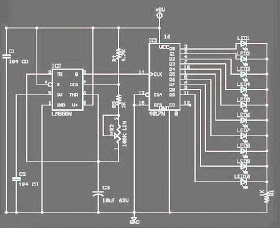
Circuit of Led runs, led can be seen using, as an indicator while ic IC4017 is that it functions as a counter with the help of a clock generated by a 555 timer ic, slow movement which quickly led the flames quickly depending on the clock late in the output by the timer IC.
Led Berjalan|Running Led

List of Components used:
  • IC 4017
  • IC Ne 555
  • Led
  • R 4.7K
  • R 1K
  • VR 100K
  • C 10mf/16V
  • C 100nf
To change the mode from the line led to the form of a text can be done with the sort led to the form of the text that will vary in, just what you want when you led or will be up on a path or line of IC 4017 should be adding a series of brace.
series brace can use here or NPN transistors can also use the relay if the load would be greater

Hukum Kirchoff Arus|Kirchoff tegangan

- Hukum Kirchoff Arus

States that "all the algebraic number of the flow enters a knot / point in the series is a zero" or "the amount of flow that enters the knot in a series with the same amount of flow that is out of the knot."
Expressed mathematically with
Hukum Kirchoff Arus

As an illustration shown in the picture below:
Hukum Kirchoff Arus

So based on the law applicable kirchof flow:
Hukum Kirchoff Arus


-Hukum Kirchoff Tegangan

States that "the amount of voltage that all algebraic corral a road closed (loop) in a series of electricity is zero." Mathematically expressed by:
Hukum Kirchoff Tegangan

As an illustration shown in the picture below:
Hukum Kirchoff Tegangan

So based on the law applicable kirchoff voltage:
Hukum Kirchoff Tegangan


-Example Kirchoff Tegangan

Determine the voltage of the unknown in the following series!
Hukum Kirchoff Tegangan

Answer:
By applying Kirchoff voltage law is
Hukum Kirchoff Tegangan

-Example Kirchoff Arus

Determine the flow of the unknown from the image below!
Hukum Kirchoff Arus

Answer:
By applying the law kirchoff flow on a point, it will be valid
Hukum Kirchoff Arus

By applying the law kirchoff flow at the point b, it will be valid
Hukum Kirchoff Arus

By applying the law kirchoff flow at the point c, it will be valid
Hukum Kirchoff Arus