Friday, March 26, 2010

Rangkaian Amplifier LA4440

This is the circuit of amplifier using IC LA4440. The amplifier circuit uses very less components but a very high quality with respect to its cost and ideal for beginners.

IC LA 4440 is wired as a bridge amplifier to deliver a 19 W Rms on a 4 Ohm speaker atau 6 W rms jika di fungsikan stereo. The IC has built in thermal over voltage and short circuit protection.The IC also incorporates a audio muting function.

Rangkaian 19 Watt Bridge Amplifier  LA4440Rangkaian 19 Watt Bridge Amplifier LA4440
Rangkaian 6 Watt Stereo Amplifier LA4440Rangkaian 6 Watt Stereo Amplifier LA4440

Note:
  • Use a 12 VDC / 3 A power supply, IC LA4440 can with stand up to 18 volts, but I prefer it should not be nothing more than 16V.
  • Do not forget to fit a proper heat sink with IC.
  • Use a 4 Ohm speaker
IC LA4440 Features
  • Built-in 2 channels enabling use in stereo and bridgeamplifier applications. (Stereo 6 Watt Bridge : 19W)
  • Minimun number of external parts required.
  • Small pop noise at the time of power supply ON/OFF and
  • good starting balance.
  • Good ripple rejection : 46dB (typ.)
  • Good channel separation.
  • Small residual noise (Rg=0).
  • Low distortion over a wide range from low frequencies to high frequencies.
  • Easy to design radiator fin.
  • Built-in audio muting function.
  • Built-in protectors.
  • Thermal protector
  • Overvoltage, surge voltage protector
  • cPin-to-pin short protector
Quick Data IC LA4440
  • Maximum supply voltage.............................18 V.
  • Allowable power dissipation Pd max............15 W.
  • Operating temperature Topr........................–20 to +75.
  • Storage temperature Tstg............................–40 to +150.
  • Voltage gain VG..........................................49.5 to 53.5.
  • Output power PO....................................... Stereo 06 W, Bridge 19 W.
  • Input resistance ri ............................. ....... 30kOhm.

Monday, March 22, 2010

Sistem Minimum Mikrokontroler AT89C51|AT89C52

The minimum system is AT89C51/AT89C52 microcontroller electronic circuits the minimum necessary to the operation of microcontroller IC. This circuit can then be connected to other circuits to perform certain functions or can be added with other complementary circuit to become a more complete system and has more functions.

Rangkaian Sistem Minimum Mikrokontroler  AT89C52|AT89C52Rangkaian Sistem Minimum Mikrokontroler
AT89C52|AT89C52

AT89S51/52 microcontroller is the latest version than the AT89C51 microcontroller has been widely used today. AT89S52 microcontroller is a CMOS 8-bit microcomputers with 8KB Flash Programmable and Erasable Read Only Memory (PEROM). Mikrokontroler tech non-volatile memory of the Atmel Cleaner density is, compatible with industry standard microcontroller MCS-51, either pin IC and the instruction set and the price is quite cheap. Therefore, it is precisely when we study this type of microcontroller.

Important specifications owned AT89S52 Microcontroller:
  • Compatible with previous MCS51 microcontroller family
  • 8 K Bytes • In system programmable (ISP) flash memory with capacity 1000 times read / write
  • 4-labor voltage 5.0V
  • Working with a range of 0 - 33MHz
  • Internal RAM 256x8 bits
  • 32 channels of I / 0 may be programmed
  • 3 pieces 16-bit Timer / Counter
  • 8 interrupt sources
  • Full duplex serial channel UART
  • watchdog timer
  • Dual data pointers
  • ISP programming mode flexible (Byte and Page Mode)

Pinning Mikrokontroler AT89C52|AT89C52Pinning Mikrokontroler AT89C52|AT89C52

Saturday, March 20, 2010

Rangkaian Downloader/Programmer AT89S51/AT89S52

Atmel is a product AT89S51/AT89S52 that quite a lot in the market with a price of less than 20 thousand rupiah. To start learning mikrokontroler type 89S51 this we need a programmer And Rangkaian Downloader. Programmer is a hardware device that is used to enter the machine language program code compilation that we write to in mikrokontroler.

Downloader AT89S51/AT89S52
Gambar Skema Rangkaian Downloader AT89S51/AT89S52

picture above shows the circuit diagram of the in-system programmer interface, the power to the interface is provided by the target system. The 74HCT541 ic isolate and buffer the parallel port signals. It is necessary to use the HCT type ic in order to make sure the programmer should also work with 3V type parallel port.

Skema rangkaian downloader ini can be use to program the 89S series devices and the AVR series devices which are pin compatible to 8051, like 90S8515. For other AVR series devices the user can make an adapter board for 20, 28 and 40 pin devices. The pin numbers shown in brackets correspond to PC parallel port
connector.

Software ISP

The ISP-30a.zip file contains the main program and the i / o port driver. Place all files in the same folder. The main screen view of the program is shown in the picture below.


Following are the main features of this software,
  • Read /write the Intel Hex file
  • Read the signature, lock and fuse bits
  • Clear/Fill memory buffer
  • Verify with memory buffer
  • Reload current Hex File
  • Display buffer checksum
  • Program selected lock bits & fuses
  • Auto detection of hardware

Decoder 4 Bit to 16 Line

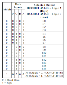
Decoder 4 bit to 16 line HCC4514B/HCC4515B are monolithic integrated circuits available in 24-lead dual in-line plastic or ceramic package and plastic micro package. The HCC/HCF4514B/4515B consisting of a 4-bit strobed latch and a 4 to 16 line decoder. The latches hold the last input data presented prior to the strobe transition from 1 to 0.Inhibit control allows all outputs to be placed at HCC/HCF4514B/4515B regardless of thestateofthedata or strobe inputs. The decode truth table indicates all combinations of data inputs and appropriate selected outputs.

Decoder 4 Bit to 16 Line HCC4514B/HCC4515B Decoder 4 Bit to 16 Line HCC4514B/HCC4515B

Absolute maximum rating HCC4514B/HCC4515B decoder 4 bit to 16 line
  • Supply Voltage: 0.5 to + 18 V
  • Input Voltage: 0.5 to VDD + 0.5 V
  • Total Power Dissipation (per package): 100 mW
  • Operating Temperature : 40 to + 85 C
  • Storage Temperature – 65 to + 150 C
Note:
Stresses above those listed under ”Absolute Maximum Ratings” may cause permanent damage to the device. This is a stress rating only and functional operation of the device at these or any other conditions above those indicated in the operational sections

decoder Logic diagramdecoder Logic diagram

truth table IC decoder HCC4514B/HCC4515Btruth table IC decoder HCC4514B/HCC4515B

3 Bit to 8 Line Demultiplexer (Dekoder)

Demultiplexer or decoders are devices that have the function desired output selection is adjusted to a predetermined input. At the decoder if input as an example of three input a1, a2 and a3, then the output will be produced 2 ^ 3 = 8 output (b1, b2, b3, b4, b5, b6, b7 and B8).

In the picture below shows an example in the specification demultiplexer using TTL IC 74HC237

demultiplexer Logic diagram 74HC237 demultiplexer Logic diagram

The 74HC237 is a 3-to-8 line demultiplexer with latches at the three address inputs The 74HC237 essentially combines the 3-to-8 decoder function with a 3-bit storage latch. When the latch is enabled (LE = LOW), the 74HC237 acts as a 3-to-8 active LOW decoder. When the latch enable (LE) goes from LOW-to-HIGH, the last data present at the inputs before this transition, is stored in the latches. Further address changes are ignored as long as LE remains HIGH.

The output enable input (E1 and E2) controls the state of the outputs independent of the address inputs or latch operation. All outputs are HIGH unless E1 is LOW and E2 is HIGH.

able IC 74HC237 demultiplexertruth table IC 74HC237 demultiplexer

IC 74HC237Pinning IC 74HC237

Quick reference data demultiplexer 74HC237
  • supply voltage: 0.5 +7 V
  • input diode current: ±20 mA
  • output diode current: ±20 mA
  • output source or sink current: ±25 mA
  • storage temperature: 65 +150 °C
  • power dissipation: 750 mW

Friday, March 19, 2010

Mode Pengalamatan ATMEL AT89S51/AT89S52

Mode Pengalamatan Microcontroller AT89S51/AT89S52

All the family members of ATMEL Microcontroller 89S51/52 have the same instruction set. This instruction set has been optimized for 8-bit control applications, and provide a variety of fast addressing modes for accessing the internal RAM and external RAM

Addressing mode 89S51/52 ATMEL Microcontroller family is as follows

Immediate Addressing

Immediate addressing is so-named because the value to be stored in memory immediately follows the operation code in memory. That is to say, the instruction itself dictates what value will be stored in memory.
Example:
  • MOV A, # 1AH ; Fill in the accumulator with data 1AH
  • MOV DPTR, # 10H ; Fill in the register DPTR with data 10H
  • MOV R1, #30H ; Fill in the register R1 with data 30H

Direct Addressing

Direct addressing is so-named because the value to be stored in memory is obtained by directly retrieving it from another memory location.
Example:
  • MOV A,15H ; Read the data Internal RAM address 15 H and store it in the Accumulator.
  • MOV 90H, A, Read the data Accumulator and store it in the SFR/Port (whose address 90H)

Indirect Addressing

In Indirect Addressing, Operands pointing to a register that contains the memory address location to be used in the operation. To implement the indirect addressing used symbol @. Addressing this type usually used for writing, transfer or reading some data in memory locations. AT89C51 has a 16-bit register (DPTR) which can be used to perform indirect addressing

Example:
  • ADD, A, R1 ; Add data internal RAM which is found at the address indicated by R1 into the data accumulator
  • DEC @ R1 ; Reduce the contents of RAM address indicated by the register R1
  • MOVX, ADPTR, A ; read data Accumulator and store it in the external memory location indicated by DPTR

Bit Addressing

Bit addressing is the appointment of bit locations address both the internal RAM or hardware using the symbol dot (.).
Example:
  • SETB p1.7; Set port 1.7 bits active
  • SETB TR1: Set TR1 (Timer 1 active)

Operator

Operators used to perform action arithmetic, logic shifting bits and others at the Operands. Some operators are available including
Arithmetic operators
  • * For multiplication
  • / For division
  • + For addition
  • - For subtraction
Example: MOV A, # 25H +3 H

Operator Logic
  • Poerasi OR to OR
  • AND to AND operation
  • XOR to XOR operations
  • EXOR for EXOR operation
  • NOT to invert operation
Example: MOV A, # 20H OR 40H; equal to MOV A, # 60H

Special Operations
  • Shr 16 ; bit shift to right
  • SHL 16 ; bit shift to the left
  • HIGH ; bits select the bag
  • LOW ; select the lower bit
  • EQ = equal to
  • NET <> ; is not equal to
  • Fl <= ; less than or equal to · GT> more
  • GE> = ; greater than or equal to

Thursday, March 18, 2010

DAFTAR INSTRUKSI PEMROGRAMAN ASSEMBLY AT89S51/S52

Kelompok Instruksi Aritmatika

ADD A,Rn (Add register to A).
ADD A, (direct Add direct byte to A).
ADD A, @Ri (Add indirect RAM to A).
ADD A,#data (Add immediate data to A).
ADDC A,Rn (Add register to A with Carry).
ADDC A (direct Add direct byte to A with Carry).
ADDC A,@Ri (Add indirect RAM to A with Carry).
ADDC A,#data (Add immediate data to A with Carry).
SUBB A,Rn (Subtract register from A with Borrow).
SUBB A,direct (Subtract direct byte from A with Borrow).
SUBB A,@Ri (Subtract indirect RAM from A with Borrow).
SUBB A,#data (Subtract immediate data from A with Borrow0).
INC A (Increment A).
INC Rn (Increment register).
INC direct (Increment direct byte).
INC @Ri (Increment indirect RAM).
DEC A (Decrement A).
DEC Rn (Decrement register).
DEC direct (Decrement direct byte).
DEC @Ri (Decrement indirect RAM).
INC DPTR (Increment Data Pointer).
MUL AB (Multiply A & B (A x B => BA)).
DIV AB (Divide A by B (A/B => A + B)).
DA A (Decimal Adjust A).


Kelompok Instruksi Logika.

ANL A,Rn (AND register to A).
ANL A,direct (AND direct byte to A).
ANL A,@Ri (AND indirect RAM to A).
ANL A,#data (AND immediate data to A).
ANL direct,A (AND A to direct byte).
ANL direct,#data (AND immediate data to direct byte).
ORL A,Rn OR (register to A).
ORL A,direct (OR direct byte to A).
ORL A,@Ri (OR indirect RAM to A).
ORL A,#data (OR immediate data to A).
ORL direct,A (OR A to direct byte).
ORL direct,#data (OR immediate data to direct byte).
XRL A,Rn (Exclusive-OR register to A).
XRL A,direct (Exclusive-OR direct byte to A).
XRL A,@Ri (Exclusive-OR indirect RAM to A).
XRL A,#data (Exclusive-OR immediate data to A).
XRL direct,A (Exclusive-OR A to direct byte).
XRL direct,#data (Exclusive-OR immediate data to direct byte).
CLR A (Clear A).
CPL A (Complement A).
RL A (Rotate A Left).
RLC A (Rotate A Left through Carry).
RR A (Rotate A Right 1 1
RRC A (Rotate A Right through Carry).
SWAP A (Swap nibbles within A).

Kelompok Instruksi Penyalinan Data.

MOV A,Rn (Move register to A).
MOV A,direct (Move direct byte to A).
MOV A,@Ri (Move indirect RAM to A).
MOV A,#data (Move immediate data to A)
MOV Rn,A (Move A to register).
MOV Rn,direct (Move direct byte to register).
MOV Rn,#data (Move immediate data to register).
MOV direct,A (Move A to direct byte).
MOV direct,Rn (Move register to direct byte).
MOV direct,direct (Move direct byte to direct byte).
MOV direct,@Ri (Move indirect RAM to direct byte).
MOV direct,#data (Move immediate data to direct byte).
MOV @Ri,A (Move A to indirect RAM).
MOV @Ri,direct (Move direct byte to indirect RAM).
MOV @Ri,#data (Move immediate data to indirect RAM).
MOV DPTR,#data16 (Load Data Pointer with 16-bit constant).
MOVC A,@A+DPTR (Move Code byte relative to DPTR to A).
MOVC A,@A+PC (Move Code byte relative to PC to A)
MOVX A,@Ri (Move External RAM (8-bit addr) to A).
MOVX A,@DPTR (Move External RAM (16-bit addr) to A)
MOVX @Ri,A (Move A to External RAM (8-bit addr))
MOVX @DPTR,A (Move A to External RAM (16-bit addr)).
PUSH direct (Push direct byte onto stack).
POP direct (Pop direct byte from stack).
XCH A,Rn (Exchange register with A).
XCH A,direct (Exchange direct byte with A).
XCH A,@Ri (Exchange indirect RAM with A).
XCHD A,@Ri (Exchange low-order Digit indirect RAM with A).

Kelompok Instruksi Bit dan Bit-test.

CLR C (Clear Carry flag).
CLR bit (Clear direct bit).
SETB C (Set Carry flag).
SETB bit (Set direct bit).
CPL C (Complement Carry flag).
CPL bit (Complement direct bit).
ANL C,bit (AND direct bit to Carry flag).
ANL C,/bit (AND complement of direct bit to Carry flag).
ORL C,bit (OR direct bit to Carry flag).
ORL C,/bit (OR complement of direct bit to Carry flag).
MOV C,bit (Move direct bit to Carry flag).
MOV bit,C (Move Carry flag to direct bit).

Kelompok Instruksi Percabangan.

ACALL addr11 (Absolute subroutine call).
LCALL addr16 (Long subroutine call).
RET (Return from subroutine).
RETI (Return from interrupt).
AJMP addr11 (Absolute Jump).
LJMP addr16 (Long Jump).
SJMP rel (Short Jump (relative addr)).
JMP @A+DPTR (Jump indirect relative to DPTR).
JZ rel (Jump if A is Zero).
JNZ rel (Jump if A is Not Zero).
JC rel (Jump if Carry flag is set).
JNC rel (Jump if No Carry flag).
JB bit,rel (Jump if direct Bit is set).
JNB bit,rel (Jump if direct Bit is Not set)
JBC bit,rel (Jump if direct Bit is set & Clear bit).
CJNE A,direct,rel (Compare direct to A & Jump if Not Equal).
CJNE A,#data,rel (Compare immediate to A & Jump if Not Equal).
CJNE Rn,#data,rel (Compare immed. to reg. & Jump if Not Equal).
CJNE @Ri,#data,rel (Compare immed. to ind. & Jump if Not Equal).
DJNZ Rn,rel (Decrement register & Jump if Not Zero).
DJNZ direct,rel (Decrement direct byte & Jump if Not Zero).
NOP (No operation).

74LS47|Decoder BCD 4-bit to Seven Segment

Decoder BCD 4-bit to Seven Segment

decoder is a logic integrated circuit which serves to show the binary codes into signals that can be responded to visual. In accordance with a variety of ways encoding, then one can find various types of decoder, which one of them to the channel decoder output BCD seven segment

Types of BCD decoder into seven segments there are two kinds namely: which decoder functions for driving seven segment common anode mode, and decoder that functions for driving seven segment common cathode mode. but in this post we only present the common cathode mode decoder using IC 74LS47. The 74LS47 is usually used to display data from counter IC which then displayed on the seven segments.

The IC 74LS47 Feature active-low outputs designed for driving common-anode seven segment leds. The Schematic diagram of the 74LS47 is used to control the seven segments in the show on the image below

Rangkaian Decoder BCD 4-bit  to Seven Segment 74LS47Skema Rangkaian Decoder BCD 4-bit to Seven Segment 74LS47


Note:
  • (BI’) must be hight “1” when output function 0 throuht 15 are desired. The (RBI’) must be hight “1” if blanking of decimal zero is not desired.
  • When (BI’) low “0” all segment outputs are off regardless of the omy other input
  • (RBI’) adn input (ABCD) are low “0” with the lamp test hight, all segment outputs go off
  • (BI/RBO’) hight and a low is applied to the lamp-test input, all segment outputa are on
for more details you can using the truth table of the IC 74LS47

Monday, March 15, 2010

60 Watt Guitar Amplifier + Tone Control

Rangkaian Guitar Amplifier + Tone Control

The following is a circuit of amplifiers are equipped with the appropriate regulatory tone in use to strengthen the electric guitar, using a single-rail supply of about 60V and capacitor-coupling for the speaker . The advantages for a guitar amplifier are the very simple circuitry, even for comparatively high power outputs, and a certain built-in degree of loudspeaker protection, due to capacitor C8, preventing the voltage supply to be conveyed into loudspeakers in case of output transistors' failure.

Rangkaian Guitar Amplifier + Tone ControlSkema Rangkaian Guitar Amplifier + Tone Control

In all cases where Darlington transistors are used as the output devices it is essential that the sensing transistor (Q2) should be in as close thermal contact with the output transistors as possible. Therefore a TO126-case transistor type was chosen for easy bolting on the heatsink, very close to the output pair

R30 must be trimmed in order to measure about half the voltage supply across the positive lead of C7 and ground. A better setting can be done using an oscilloscope, in order to obtain a symmetrical clipping of the output wave form at maximum output power

Note:
To set quiescent current, tide ampare meter in series between supplay with this series, then do the following
  • Set the volume control to the minimum and Trimmer R3 to its minimum resistance.
  • Power-on the circuit and adjust R3 to read a current drawing of about 30 to 35mA.
  • Wait about 15 minutes, watch if the current is varying and readjust if necessary.

List component

R1,R2______________68K 1/4W Resistors
R3________________680K 1/4W Resistor
R4________________220K 1/4W Resistor
R5_________________33K 1/4W Resistor
R6,R16______________2K2 1/4W Resistors
R7__________________5K6 1/4W Resistor
R8,R21____________330R 1/4W Resistors
R9_________________47K 1/4W Resistor
R10_______________470R 1/4W Resistor
R11_________________4K7 1/4W Resistor
R12,R20____________10K 1/4W Resistors
R13_______________100R 1/4W Resistor
R14,R15____________47R 1/4W Resistors
R17,R18,R19_______100K 1/4W Resistors
R22__________________6K8 1W Resistor
R23,R25_____________470R 1/4W Resistors
R24__________________2K 1/2W Trimmer Cermet
R26,R27_______________4K7 1/2W Resistors
R28________________220R 1/2W Resistor
R29__________________2K2 1/2W Resistor
R30_________________50K 1/2W Trimmer Cermet
R31________________68K 1/4W Resistor
R32,R33______________R47 4W Wirewound Resistors


C1,C4,C5,C6________10µF 63V Electrolytic Capacitors
C2_________________47µF 63V Electrolytic Capacitor
C3_________________47pF 63V Ceramic Capacitor
C7_________________15nF 63V Polyester Capacitor
C8_________________22nF 63V Polyester Capacitor
C9________________470nF 63V Polyester Capacitor
C10,C11,C12________10µF 63V Electrolytic Capacitors
C13_______________220µF 63V Electrolytic Capacitor
C14,C15,C17,C18________47µF 63V Electrolytic Capacitors
C16________________100µF 25V Electrolytic Capacitor
C19_________________33pF 63V Ceramic Capacitor
C20_______________1000µF 50V Electrolytic Capacitor

P1,P2______________10K   Potentiometers
P3_________________10K Potentiometer

D1,D2____________BAT46 100V 150mA Schottky-barrier Diodes
D3_________________LED

Q1,Q3____________BC546 NPN Transistors
Q2_______________BC556 PNP Transistor
Q4,Q5____________BD139 80V 1.5A NPN Transistors
Q6_____________MJ11016 120V 30A NPN Darlington Transistor
Q7_____________MJ11015 120V 30A PNP Darlington Transistor

J1,J2___________6.3mm. Mono Jack sockets
SW1,SW2___________SPST Switches
SPKR______________speakers 8 or 4 Ohm with Minimum power 75W

Rangkaian Decoder Seven Segmen 5 Bit

This decoder circuit also serves to change the 5-bit binary numbers to decimal to be displayed by seven segments. This decoder has a 5 pin input PA, PB, PC, PD PE and 14 pin output marked a, b, c, d, e, f and g.

For example, if the input PA, PB, PC, PD, PE = 11 01 0, then after the translated by the decoder will produce numbers a, b, c, d, e, f, g (MSD) = 10 0 1 1 1 1 and a, b, c, d, e, f, g (LSB) = 0 0 1 0 0 1 0. These numbers indicate that the negative pole (cathode) of the LED in a particular segment of a low voltage bias (0) so that the lights forming the number "12" on the seven-segment display devices. For more details can be seen in the picture

Rangkaian Decoder Seven Segmen 5 BitRangkaian Decoder Seven Segmen 5 Bit

In the circuit above using Seven Segment (7 Segment ) commond anode type. The principle works is, if the input pin Seven Segment a, b, c, d, e, f, g given voltage 0 volts, the LED on the Seven Segment props will be forward biased and turned to form a specific figure.

The seven segments can also be supplied with higher voltage (up to 18 V) but you have to replace the R 22 ohm with a greater value; morever, a suitable mast Rext be Chosen

Here is the truth table of the IC TDA4092 decoder

Absolute maximum rating IC TDA4092
  • Supply voltage…………….... 10 V
  • Input voltage……………….. .10 V
  • Off state output voltage…...... 20 V
  • Output current………………. 22 V
  • Total power dissipation ….. ... 0.8 mW
  • Storage and junction storage… -25 to 150 C
  • Operating temperature………. 0 to 70 C

Thursday, March 04, 2010

Rangkaian Dimmer (Pengatur Contras Lampu 220V)

Dimmers circuit useful to control the lighting of a lamp level (brightness control) by regulating voltage Vrms (root mean square voltage). Most Interior or Lighting Design Consultant must include dimmers on each of their design, because their system with dimmers can regulate mood and color of a room with more perfect.

Rangkaian Dimmer (Pengatur Contras Lampu 220V)Skema Rangkaian Dimmer (Pengatur Contras Lampu 220V)

dimmer circuit graph

This circuit is typical of a high-end leading-edge dimmers. C1 and L1 are for RF interference suppression. The circuit operates by utilising the phase shift created by VR1, C2, R1 and C3. This network delays the signal applied to DB1 (a bidirectional breakdown diode called a DIAC). When the voltage exceeds the 30V (typical) breakdown voltage of the DIAC, it Conducts fully and the charge in C3 is used to trigger the TRIAC. Once triggered, the triac will conduct fully until the current falls to near zero, at which time it turns off again. This process is repeated for every half-cycle of the mains voltage. The delay, turn-on and turn-off points are visible and indicated in the graph above.

Leading edge dimmers must never be used with a capacitive load (most electronic ballast circuits), because the very fast rise time of the voltage causes extremely high instantaneous current flow into the capacitor. Inductive loads (such as conventional iron-core transformers) are quite safe, since the inductance limits the rise time of the current to safe values.

Tuesday, March 02, 2010

Rangkaian Power Amplifier Sound System 2000 Watt

This power amplifier circuit provides up to 2000Watt, it has to be said that this amplifier will blow up any speaker connected to it. I recommend this as a 'thought experiment', rather than actually doing it!. 110V RMS into 8 ohms is 1500 W. How long would you expect the speaker to last? Most will be toast within perhaps 30 seconds or less!

Rangkian Power Amplifier 2000 WattSkema rangkaian power amplifier sound system 2000 watt

The transistor Q5 (the bias servo transistor) is mounted on the heatsink, in excellent thermal contact. This is because, unlike most of my other designs, this amp uses conventional Darlington output configuration. It is necessary to use a Darlington arrangement (or a low power Darlington transistor as shown) for Q5 to ensure that the bias remains at a safe value with temperature. There is probably good cause to model and test this aspect of the design very carefully, because it is so important. The arrangement as shown will reduce quiescent current at elevated temperatures. For example, if total Iq at 24°C is 165mA, this will fall to ~40mA at 70°C. This is probably fine, because there is some delay between the a power 'surge' and the output transistors transferring their heat to the bias servo via the heatsink.

The power supply needed for an amp of this size is massive. Grown welding machines will look at it and cry. For intermittent operation, you need a minimum of a 1000VA transformer (or 1500VA for the 2000W version), and it will have to be custom made because of the voltages used. If you expect to run the amp at continuous high power, then transformers should be 2kVA and 3000VA respectively. Filter capacitors will pose a problem - because you need caps rated for 150V, these will be hard to find. Because high voltage high value caps can be difficult to find, it may be necessary to use two electros in series for each capacitor location. This is the arrangement shown. You must include the resistors in parallel - these equalise the voltage across each capacitor so that they have the same voltage. Remember to verify the ripple current rating! This can be expected to be over 10A, and under-rated capacitors will blow up.

Skema Rangkaian Power Supplay 2000 VA

WARNING

This project describes an amplifier, power supply and tests procedures that are all inherently dangerous. Nothing described in this article should even be considered unless you are fully experienced, know exactly what you are doing, and are willing to take full 100% responsibility for what you do. There are aspects of the design that may require analysis, fault-finding and/or modification

Source

Rangkaian Audio Signal Injector|Tracer

This circuit can be used as a signal injector or signal tracer. This circuit is very helpful in trouble shooting audio circuits, when you need to test a circuit by injecting a signal and observe the output (by watching the oscilloscope or by hearing the loudspeaker ), or by tracing some points inside the circuit when an audio signal is applied to the input.

Rangkaian Audio Signal Injector|TracerSkema Rangkaian Audio Signal Injector|Tracer

The circuit uses supply from 9 volts battery. An alligator clip is recommneded for the ground probes, so you can works with one hand to hold the board, and the other hand to target the test probes. The SPDT switch connected to the transitor and the earpiece is used to select the function, whether as a signal or a signal injector tracer.


Transistor 2n3904

This transistor is designed as a general purpose amplifier and switch. The useful dynamic range extends to 100 mA as a switch and to 100 MHz as an amplifier.
Transistor 2n3904 Pin

Absolute maximum rating
  • Collector-Emitter Voltage 40 V
  • Collector-Base Voltage 60 V
  • Emitter-Base Voltage 6.0 V
  • Collector Current - Continuous 200 mA
  • Operating and Storage Junction Temperature Range -55 to +150 °C

Monday, March 01, 2010

Rangkaian Pengukur Induktansi (Inductance Meter)

Inductor

An inductor is a passive electronic component that can store energy in magnetic fields generated by electric current through it. Inductor's ability to store magnetic energy is determined by induktansinya

Inductance (L) (measured in Henry) is the effect of the magnetic field formed around the current carrying conductor that is holding the current changes. The electric current through the conductor makes the magnetic field is proportional to the magnitude of the flow. Changes in the flow causes the magnetic field changes that result in the opposite electromotive force induced by GGL that are against changing the current.

Rangkaian Pengukur Induktansi (Inductance Meter )

This inductance meter is capable of measuring inductor value. Inductance meter is very helpful in designing coil by hand and measure the inductance from trial and error to get the required value. The Inductance meter is designed to provide twi measurement range. The low range will measure inductors with inductance value between 3uH to 500uH, and the high range will measure inductance values between 100uH and 5mH.

Rangkaian Pengukur Induktansi
Skema Rangkaian Pengukur Induktansi

To calibrate this inductance meter adapter, connect a digital voltmeter, swith the voltmeter to 200 mV range, short the test probe and adjust the zero (R1) to give zero millivolt reading on your digital voltmeter. To calibrate the low range of this inductance meter adapter, switch the voltmeter to low range position, and select 2 V range for the digital voltmeter. Test a known inductor that has value around 400uH, adjust the low calibration pot to give correct reading of 1mV / uH. If you use a 400uH inductor then you must adjust the calibration to give exactly a 400mV reading. For high range calibration, switch the range selector to high position and use a known inductor around 5 mH, adjust the high calibration pot to give 100mV per mH. A 5 mH inductor should give a 500mV reading on your DVM.