Thursday, February 26, 2009

HEXFET® Power MOSFET

IRF Z44N


Description

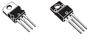
Advanced HEXFET® Power MOSFETs from International Rectifier utilize advanced processing techniques to achieve extremely low on-resistance per silicon area. This benefit, combined with the fast switching speed and ruggedized device design that HEXFET power MOSFETs are well known for, provides the designer with an extremely efficient and reliable device for use in a wide variety of applications. The TO-220 package is universally preferred for all commercial-industrial applications at power dissipation levels to approximately 50 watts. The low thermal resistance and low package cost of the TO-220 contribute to its wide acceptance throughout the industry.

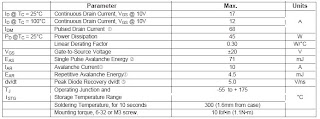
Absolute Maximum Ratings


Notes:
  • Repetitive rating; pulse width limited by max. junction temperature.
  • Starting TJ = 25°C, L = 0.48mH RG = 25W, IAS = 25A.
  • ISD £ 25A, di/dt £ 230A/μs, VDD £ V(BR)DSS, TJ £ 175°C.
  • Pulse width £ 400μs; duty cycle £ 2%.
  • This is a typical value at device destruction and represents operation outside rated limits.
  • This is a calculated value limited to TJ = 175°C .

IRF Z44N


Description

Fifth Generation HEXFET® power MOSFETs from International Rectifier utilize advanced processing techniques to achieve the lowest possible on-resistance per silicon area. This benefit, combined with the fast switching speed and ruggedized device design that HEXFET power MOSFETs are well known for, provides the designer with an extremely efficient device for use in a wide variety of applications. The TO-220 package is universally preferred for all commercial-industrial applications at power dissipation levels to approximately 50 watts. The low thermal resistance and low package cost of the TO-220 contribute to its wide acceptance throughout the industry.

Absolute Maximum Ratings


Notes:
  • Repetitive rating; pulse width limited by max. junction temperature.
  • VDD = 25V, starting TJ = 25°C, L = 1.0mH RG = 25W, IAS = 10A.
  • ISD £ 10A, di/dt £ 280A/μs, VDD £ V(BR)DSS, TJ £ 175°C
  • Pulse width £ 300μs; duty cycle £ 2%.

IRF Z48N


Description

Advanced HEXFET® Power MOSFETs from International Rectifier utilize advanced processing techniques to achieve extremely low on-resistance per silicon area. This benefit, combined with the fast switching speed and ruggedized device design that HEXFET power MOSFETs are well known for, provides the designer with an extremely efficient and reliable device for use in a wide variety of applications. The TO-220 package is universally preferred for all commercial-industrial applications at power dissipation levels to approximately 50 watts. The low thermal resistance and low package cost of the TO-220 contribute to its wide acceptance throughout the industry.

Absolute Maximum Ratings


NOTES:
  • Repetitive rating; pulse width limited bymax. junction temperature.
  • Starting TJ = 25°C, L = 0.37mH RG = 25W, IAS = 32A.
  • ISD £ 32A, di/dt £ 220A/μs, VDD £ V(BR)DSS, TJ £ 175°C
  • Pulse width £ 400μs; duty cycle £ 2%.
  • This is the destructive value not limited to the thermal limit.
  • This is the thermal limited value.

READMORE...

Thursday, February 19, 2009

ADAPTOR 12 VOLT 20 AMPERE

Now it should not have to wrestle again seek op-amp, transistor and other components to realize a massive circuit of regulators, because the circuit of this kind have been packed into a fixed voltage regulator IC. Currently, many components known as the 78XX series fixed positive voltage regulator and the 79XX series is a voltage regulator to remain negative.

Even the components are usually already equipped with a flow divider (current limiter) and also the constraint temperature (thermal shutdown). This component is only three pins, and by adding some components can only have a circuit of ration power ter-regulation with either.

For example, 7805 is a voltage regulator to get a 5 volt, 7812 voltage regulator 12 volt, and so on, for example, while the 79XX series is the 7905 and 7912 respectively are negative voltage regulators 5 and 12 volt.


RANGKAIAN ADAPTOR 12 VOLT


The adapter has a set of outputs (output) 12 volt which is teregulasi well. If the components that were installed in accordance with the scheme under the set of the circuit of this adapter safe burdened to 5 ampere, if you want this adapter is able to provide a greater flow you can add a power transistor (2N3055) and replace the bridge diode with diode which has a more ampere high. Exodus circuit of this adapter can be used to run the tape the car, the radio transmitter, CCTV cameras, and other electronics equipment.
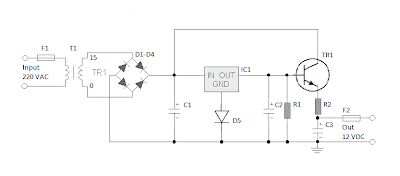
Circuit of adapter 12 voltGbr. Skema rangkaian adaptor 12 volt, 5 ampere

List of components adapter 12 volt:
  • D1-D4 = 6 A
  • D5 = 1 A
  • C1 = 4700u/50V
  • C2 = 220u/25V
  • C3 = 100u/25V
  • R1 = 1k
  • R2 = 0.2Ohm/5Watt
  • F1 = Fuse (skring) 2 A
  • F2 = Fuse (skring) 6 A
  • IC1 = 7812
  • TR1 = 2N3055
  • T1 = Trafo 15Volt/5A
Scheme following a circuit of adapter has the ability to supply higher current (20 ampere is reached). For fans radio transmitter (radio station) following a circuit of adapter is suitable to use. Provide a good cooling on the power transistor (MJ 2955) because the transistor will be very hot when the adapter to provide a large flow.

Circuit of adapter 12volt, 30A
Skema Rangkaian adaptor 12Volt/ 20 ampere

READMORE...

Friday, February 13, 2009

Rangkaian Regulator IC 79xx (7905,7912,7915...)

The available voltage from a voltage source that is usually not appropriate to the needs. It is necessary for a voltage regulator that functions to maintain the constant voltage value on a certain value. Voltage regulator chip is usually a code with the 78xx or 79xx. For the 79xx series is used for DC negative voltage regulator. xx indicates the regulator output voltage. For example, the system needs is a -5 volt negative, the regulator used is 7905. Chip regulator consists of three pins, namely input, output and ground. In this IC uses the input voltage must be greater several percent (depending on the data sheet) from the value output voltage.


Fisik 79xx
physical 79xx regulator chip

Pin Ic 79xx

data sheet 79xx
data sheet 79xx

READMORE...

Sunday, February 08, 2009

Rangkaian Regulator 78xx (7805,7812,7815...)

The available voltage from a voltage source that is usually not appropriate to the needs. It is necessary for a voltage regulator that functions to maintain the constant voltage value on a certain value. Voltage regulator chip is usually a code with the 78xx or 79xx. For the 78xx series is used for DC positive voltage regulator. xx indicates the regulator output voltage. For example, the system needs is a + 5 volt positive, the regulator used is 7805. Chip regulator consists of three pins, namely input, output and ground. In this IC uses the input voltage must be greater several percent (depending on the data sheet) from the value output voltage.
search

Chip lm78xx provide facilities in the affairs regulator. price is also relatively inexpensive and easy to find in the market

body Regulator 78xx

Features important in the IC LM 78xx:
  • current up to 1A
  • Security short internal
  • Safe temperatures 0°C - 70°C
  • Temperature max 150°C

Voltage out put in the offer:
  • LM7805C 5V
  • LM7806c 6V
  • LM7808 8V
  • LM7809 9V
  • LM 7810 10V
  • LM7812C 12V
  • LM7815C 15V
  • LM7824 24V
To be able to work with both the input voltage must be greater (voltage output volt + 3) of the output voltage. Example of the 7812 then bisanya skitar input voltage 15v

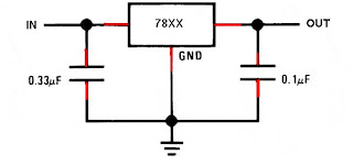
Rangkaian 78xxSkema Rangkaian 78 xx

READMORE...

Saturday, February 07, 2009

TRANSISTOR POWER 2N3055|MJ2955

Transistor ini biasa di gunakan pada power (amplifier) tingkat menengah
Fitur:

  • Arus colektor - emitor max 15 Ampere
  • Disipasi daya max 115 watt
  • teganngan Colektor- emitor max 60 volt
  • penguatan arus (hfe) 20-70
Bentuk fisik transistor 2N3055/MJ2955


READMORE...

DIODA ZENER

Phenomena tegangan breakdown dioda ini mengilhami pembuatan komponen elektronika lainnya yang dinamakan zener. Sebenarnya tidak ada perbedaan sruktur dasar dari zener, melainkan mirip dengan dioda. Tetapi dengan memberi jumlah doping yang lebih banyak pada sambungan P dan N, ternyata tegangan breakdown dioda bisa makin cepat tercapai. Jika pada dioda biasanya baru terjadi breakdown pada tegangan ratusan volt, pada zener bisa terjadi pada angka puluhan dan satuan volt. Di datasheet ada zener yang memiliki tegangan Vz sebesar 1.5 volt, 3.5 volt dan sebagainya.

Simbol Zener

Ini adalah karakteristik zener yang unik. Jika dioda bekerja pada bias maju maka zener biasanya berguna pada bias negatif (reverse bias).


READMORE...

LED (Light Emiting Dioda)

LED (Light Emiting Dioda), is a component can product of emissions light. LED findings after dioda. With the same structure also dioda, but later found that the electrons that run into the connection PN also release energy as heat energy and light energy. LED is made to be more efficient if the light issue. To produce light emissions in the semiconductor, doping is the use galium, arsenic and phosporus. A different type of doping will produce a different color of light also.
symbol LED

At this time the colors of LED that there is a lot of red, yellow and green. Basically, all colors can be produced, but it will be very expensive and inefficient.

READMORE...

Friday, February 06, 2009

Data Sheet transistor Fet UPS

Transistor fet ini sering di gunakan pada ups-ups yang beredar di pasaran. tapi sayangnya agat sukar mendapatkan suku cadang jenis ini.


READMORE...

JAM DIGITAL Menggunakan Gerbang Dasar

Rangkaian jam digital dibentuk dari rangkaian pencacah serta pembangkit detak 1 detik. Pulsa-pulsa dengan lebar 1 detik dicacah oleh pencacah yang bertingkat dari detik satuan, detik puluhan, menit satuan, menit puluhan, jam satuan serta jam puluhan. Setiap hasil cacahan kemudian ditampilkan menggunakan led tujuh ruas. Gambar 1 berikut adalah rangkaian pencacah untuk besaran detik dan menit.

Gambar Rangkaian pencacah besaran detik


Rangkaian pencacah detik dan menit bekerja untuk menghitung banyaknya detik dan menit. Rangkaian ini terdiri dari dua tingkat yaitu satuan dan puluhan menggunakan komponen utama IC 74LS393. Untuk tingkat satuan, pencacah bekerja pada modulo 10, sedangkan untuk tingkat puluhan, pencacah bekerja pada modulo 6.

Gambar Rangkaian pencacah besaran jam.

Untuk rangkaian pencacah jam, rangkaian ini terdiri dari dua tingkat pencacah yaitu untuk pencacah jam satuan serta puluhan menggunakan komponen utama IC 74LS197. IC ini merupakan pencacah biner yang dapat dimuati dengan nilai awal. Kedua tingkat pencacah ini bekerja pada modulo 12, dengan nilai terendah adalah 1 serta nilai tertinggi adalah 12. Kondisi ini dapat dicapai dengan memuati pencacah dengan nilai 0 1 ketika hasil cacahan pada angka 13.

READMORE...

Wednesday, February 04, 2009

TRANSISTOR

Fungsi utama transistor adalah sebagai penguat sinyal dan sebagai saklar elektronik. Dibandingkan dengan Tabung Hampa, transistor mempunyai kelebihan antara lain bentuk fisiknya yang lebih kecil dan daya yang digunakan lebih kecil.


Gambar fisik transisitor

Secara tipikal transistor mempunyai tiga pin, yaitu:

  • Basis
  • Emitor
  • Kolektor

Basis merupakan pin untuk meng-aktifkan dan meng-non-aktifkan sebuah transistor. Emitor dan kolektor dihubungkan ke sumber tegangan positif atan negatif atau ground (tergantung konfigurasi transistor).

Transistor terbagi menjadi dua tipe yaitu NPN dan PNP. Untuk membedakan transistor tipe NPN atau PNP, kamu bisa lihat di tanda panah pada kaki emitornya ( di gambar rangkaiannya lo ya, bukan bentuk fisiknya ). Untuk NPN arah panahnya keluar, sedangkan untuk PNP arah panahnya kedalam Lihat gambar 3 saja, biar lebih jelas.

Gambar Simbol Transistor

Untuk menentukan kaki Basis Emitor Kolektor dari sebuah transistor biasanya digunakan multimeter. Tetapi saya punya beberapa tips untuk menentukan kaki transistor tanpa menggunakan multimeter, caranya adalah :

  • Kaki kolektor biasanya terhubung dengan badan transistor apabila transistor tersebut dipacking menggunakan metal. Apabila transistor dipacking dengan plastik maka kaki kolektor biasanya terhubung dengan badan transistor yang akan dihubungkan dengan pendingin.
  • Apabila transistor tersebut tidak dihubungkan dengan pendingin, maka sebaiknya dicari dulu kaki basisnya. Kalau sudah ketemu, sekarang kaki basisnya ditengah apa dipinggir? Kalau kaki basisnya ditengah, biasanya kaki kolektor berada pada sebelah kanan. Kalau basisnya dipinggir maka kaki kolektor berada pada sebelah tengah.

Gambar Konfigurasi Kaki Transistor


Cara menentukan Kaki Basis transistor dengan multimeter :


Gambar Cara menentukan kaki basis transistor
  • Atur multimeter pada pengukuran ohmmeter x100.
  • Lakukan pengukuran seperti gambar diatas.° Perhatikan penunjukkan pergerakan jarum.
  • Apabila jarum bergerak ke kanan dengan posisi probe yang satu tetap pada kaki 3 dan probe lainnya pada kaki 1 atau kaki 2 berarti kaki 3 adalah basis transistor. Jika probe negatif yang berada pada kaki 3 berarti transistor tersebut berjenis NPN, sebaliknya jika probe positif berada pada kaki 3 berarti transistortersebut berjenis PNP.
Cara menentukan Kaki Kolektor dan Emitter


Gambar Cara menentukan kaki emiter dan kolektor transistor
  • Misal: transistor berjenis NPN
  • Lakukan pengukuran seperti gambar diatas.
  • Perhatikan penunjukkan jarum, apabila jarum bergerak ke kanan maka kaki 1 (pada probe negatif) adalah emitter dan kaki 2 (pada posisi probe positif) adalah kolektor. Atau jika dipasang kebalikkannya (probe negatif pada kaki 2 dan probe positif pada kaki 1) dan jarum tidak bergerak, maka kaki 1 adalah emitter dan kaki 2 adalah kolektor.
  • Untuk transistor jenis PNP dapat dilakukan seperti diatas dan hasilnya kebalikan dari transistor jenis NPN.

READMORE...
 
Skema Rangkaian Elektronika