Wednesday, September 30, 2009

Rangkaian Pendeteksi Metal

This is a metal detector circuit used IC CS209A . A 100uH coil is used to sense the presence of metal. The IC CS209A has a built in oscillator circuit and the coil L1 forms a part of its external LC circuit which determines the frequency of oscillation. The inductance of the coil change in the presence of metals and the resultant change in oscillation is demodulated to create an alarm. The LED gives a visual indication too. This circuit can sense metals up to a distance of few inches.

Pendeteksi Metal
Skema Rangkaian Pendeteksi Metal


Note:
The switch S1 can be a slide type ON/OFF switch.
The POT R1 can be used to adjust the sensitivity of the circuit.


IC CS209A Description

The CS209A is a bipolar monolithic integrated circuit for use in metal detection (Pendeteksi Metal)/ proximity sensing applications. The IC (see block diagram) contains two on-chip current regulators, oscillator and low-level feedback circuitry, peak detection/demodulation circuit, a comparator and two complementary output stages.

The oscillator, along with an external LC network, provides controlled oscillations
where amplitude is highly dependent on the Q of the LC tank. During low Q conditions, a variable low-level feedback circuit provides drive to maintain oscillation. The peak demodulator senses the negative portion of the oscillator envelop and provides a demodulated waveform as input to the comparator. The comparator sets the states of the complementary outputs by comparing the input from the demodulator to an internal reference. External loads are required for the output pins. A transient suppression circuit is included to absorb negative transients


Lay out IC CS209A and diagram blog IC CS209A


Absolute Maximum Ratings
Supply Voltage ................................................................................................24V
Power Dissipation (TA = 125¡C).............................................................200mW
Storage Temperature Range ....................................................Ð55¡C to +165¡C
Junction Temperature...............................................................Ð40¡C to +150¡C
Electrostatic Discharge (except TANK pin) ................................................2kV
Lead Temperature Soldering
Wave Solder(through hole styles only) ...........10 sec. max, 260¡C peak
Reflow (SMD styles only) ...........60 sec. max above 183¡C, 230¡C peak

READMORE...

Friday, September 25, 2009

Rangkaian Pre-Amp Sepul Gitar

This is a pre-amp guitar circuit suitable for high impedance type electric guitar pickups. The circuit is based on a uA 741 op-amp (IC1). The IC1 is wired as a non-inverting amplifier. Resistor Variable R1 can be used as a volume controller. Resistor Variable R6 can be used as tone controller. The switch S1 is used to produce “brilliant” or “soft” tonal effects.

Pre-Amp Sepul Gitar

Skema rangkaian Pre-Amp sepul gitar

Description Op-Amp UA741

The UA741 is a high performance monolithic operational amplifier constructed on a single silicon chip. It is intented for a wide range of analog applications.

* Summing amplifier
* Voltage follower
* Integrator
* Active filter
* Function generator

The high gain and wide range of operating voltages provide superior performances in integrator, summing amplifier and general feedback applications. The internal compensation network (6dB/ octave) insures stability in closed loop circuits.

Data max Ic UA741

* Symbol Parameter UA741M UA741I UA741C Unit
* Supply voltage (VCC) ±22 V
* Differential Input Voltage (Vid ) ±30 V
* Input Voltage (Vi ) ±15 V
* Power Dissipation (Ptot) 500 mW
* Storage Temperature Range (Tstg) -65 to +150 °C.

READMORE...

Thursday, September 24, 2009

Rangkaian Bell Pintu Rumah

This is a doorbell circuit use IC NE555.When some one presses switch S1 momentarily, the loud speaker sounds a bell tone as long as the time period of the monostable multivibrator (IC1). When the switch S1 pressed, IC1 is triggered at its pin 2 and output pin 3 goes high for a time period previously set by the values of POT R4 and POT R5.When the output of IC1 goes high it resets IC2 and it starts to oscillate to make a bell sound through the speaker.The IC2 is configured as an astable multivibrator whose oscillation frequency can be varied with the help of POT R5.By adjusting the values of R4 & R5, modifications on the tone are possible.

Bell PintuSkema rangkaian bell pintu


IC NE555 description

The NE555 monolithic timing circuit is a highly stable controller capable of producing accurate time delays or oscillation. In the time delay mode of operation, the time is precisely controlled by one external resistor and capacitor. For a stable operation as an oscillator, the free running frequency and the duty cycle are both accurately controlled with two external resistors and one capacitor. The circuit may be triggered and reset on falling waveforms, and the output structure can source or sink up to 200mA. The NE555 is available in plastic and ceramic minidip package and in a 8-lead micropackage and in metal can package version.

Lay out and diagram IC NE555


Pin connnections IC NE555

1 - GND
2 - Trigger
3 - Output
4 - Reset
5 - Control voltage
6 - Threshold
7 - Discharge
8 – VCC

Absolute maximum ratings
Supply Voltage: 18 V
Operating Free Air Temperature Range for NE555: 0 to 70 oC
Junction Temperature 150 oC
Storage Temperature Range –65 to 150 oC.
.

READMORE...

Rangkaian Penerima Radio Fm Sederhana

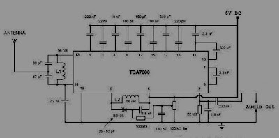
Here is a FM radio circuit using IC7400. IC TDA7000 is a monolithic integrated circuit for mono FM portable radios, where a minimum on peripheral components is crucial. The IC TDA7000 has a Frequency-Locked-Loop system with an intermediate frequency of 70 kHz. The intermediate frequency selectivity is achieved by active RC filters. The only function which needs alignment is the resonant circuit for the oscillator, thus selecting the reception frequency. Spurious reception is avoided by means of a mute circuit, which also eliminates too noisy input signals. Special steps are taken to meet the radiation requirements

Penerima Radio FmSkema Rangkaian Penerima Radio Fm


• L1 and L2 wind 5 turns of 0.6 mm enameled Copper wire on a 4 mm dia plastic former.


IC TDA7000 Description

The TDA7000 is a monolithic integrated circuit for mono FM portable radios, where a minimum on peripheral components is important (small dimensions and low costs).
The IC has an FLL (Frequency-Locked-Loop) system with an intermediate frequency of 70 kHz. The i.f. selectivity is obtained by active RC filters. The only function which needs alignment is the resonant circuit for the oscillator, thus selecting the reception frequency. Spurious reception is avoided by means of a mute circuit, which also eliminates too noisy input signals. Special precautions are taken to meet the radiation requirements.

IC TDA7000Lay out IC TDA7000


Data IC TDA7000

Supply voltage range: 2,7 to 10 V
Supply current : 8 mA
R.F. input frequency range: 1,5 to 110 MHz
Sensitivity for -3 dB limiting
• (e.m.f. voltage)
• (source impedance: 75 Ohm mute disabled) EMF: 1,5 uV
Signal handling (e.m.f. voltage)
• (source impedance: 75 Ohm) EMF typ. 200 mV
A.F. output voltage at RL = 22 kOhm75 Mv

Supply voltage: max. 12 V
Oscillator voltage: 0,5 to VP0,5 V
Storage temperature 55 to 150 C
Operating ambient temperature 0 to 60 C.
.

READMORE...

Wednesday, September 23, 2009

Rangkaian Sensor Parkir Mobil

This is circuit can be used for sensing the distance between the rear bumper of the car and any obstacle behind the car. The distance can be understood from the combination of the LEDs (D5 to D7) glowing. At 25cm D7 will glow, at 20 cm D7&D6 will glow and at 5cm D7, D6 and D5 will glow. When the obstacle is beyond 25 cm none of the above LEDs will glow.

Sensor Parkir MobilSkema rangkaian receiver sensor parkir mobil


Sensor Parkir MobilSkema rangkaian transmitter sensor parkir mobil


Note:
  • D1 & D2 must be mounted close (~2cm)
  • D1 can be a general purpose IR LED.
  • D2 can be general purpose IR photo diode with sun filter.
  • Transmitter as well as receiver can be powered from the car battery.
  • For proper working of the circuit, some trial and error is needed with the position of D1 and D2 on the dash board.


Two ICs are used in the circuit. The IC1 (NE555) is wired as an astable multivibrator for driving the IR Diode D1 to emit IR pulses. The operating frequency of the transmitter is set to be 120Hz.The IR pulses transmitted by D1 will be reflected by the obstacle and received by the D2 (IR photo diode).The received signal will be amplified by IC2a.The peak of the amplified signal will be detected by the diode D4 and capacitor C4.R5 and R6 compensates the forward voltage drop of D4.The output voltage of the peak detector will be proportional to the distance between car’s bumper and obstacle. The output of peak detector is given to the inputs of the other three comparators IC2b,IC2c and IC2d inside the IC2(LM324).The comparators switch the status LEDs according to the input voltage their inverting inputs and reference voltages at their non inverting inputs. Resistances R7 to R10 are used to set the reference voltages for the comparators.


Lay out IC LM324
 Lay out IC LM324
Features

Internally frequency compensated for unity gain
Large DC voltage gain 100 dB
Wide bandwidth (unity gain) 1 MHz (temperature compensated)
Wide power supply range:Single supply 3V to 32V or dual supplies ±1.5V to ±16V
Very low supply current drain (700 μA)—essentially
independent of supply voltage
Low input biasing current 45 nA (temperature compensated)
Low input offset voltage 2 mV and offset current: 5 nA
Input common-mode voltage range includes ground
Differential input voltage range equal to the power supply voltage
Large output voltage swing 0V to V+ − 1.5V.
.

READMORE...

Rangkaian 100 watt Sub-Woofer Amplifier

This is the circuit of subwoofer amplifier. This amplifier can produce an output of 100Watt. There are seven transistors including four in the output stage. The transistors Q1 and Q2 form the preamplifier stage. Transistors Q4 to Q7 form the output stage. Since no ICs are used the circuit is very robust and can be easily assembled on a general purpose PCB.
100 watt sub-woofer amplifierSkema rangkaian 100 watt sub-woofer amplifier

Note:
Use powered a +35V/-35V, 5A dual power supply.
All electrolytic capacitors must be rated 100V.
The transistor Q4 to Q7 must be fitted with heat sinks.


Transistor 2N3773 and 2N6609

Transistor 2N3773 (NPN) and (PNP) 2N6609 are PowerBase_ power transistors designed for high power audio, disk head positioners and other linear applications. These devices can also be used in power switching circuits such as relay or solenoid drivers, DC−DC converters or inverters.

Transistor 2N3773
Features Transistor 2N3773

Pb−Free Packages are Available
High Safe Operating Area (100% Tested) 150 W @ 100 V
Completely Characterized for Linear Operation
High DC Current Gain and Low Saturation Voltage
hFE = 15 (Min) @ 8.0 A, 4.0 V
VCE(sat) = 1.4 V (Max) @ IC = 8.0 A, IB = 0.8 A
For Low Distortion Complementary Designs


MAXIMUM RATINGS Transistor 2N3773

Collector − Emitter Voltage: 140 Vdc
Collector − Emitter Voltage: 160 Vdc
Collector − Base Voltage:160 Vdc
Emitter − Base Voltage: 7 Vdc
Collector Current Continuous: 16 Adc
Base Current Continuous 15 Adc
Total Power Dissipation : 150 Watt.
.

READMORE...

Tuesday, September 22, 2009

Osilator Gelomabang Kotak varibel 1Hz-10Khz

This is a Circuit of square wave generator using IC uA741. The circuit uses positive feedback for Schmitt trigger action and negative feedback for timing of the wave form.


Let us presume that the output is high and the capacitor C1 is fully discharged.C1 now starts charging via R2 and R1. When the voltage across C1 rises above that the Junction of R3 & R4,the output quickly switches to fully negative voltage.C1 now starts discharging and charges in the opposite direction.Again,when the negative voltage across C1 falls below that at pin 3,the circuit switches back quickly to the fully positive output value.The cycle repeats endlessly.

Osilator Gelomabang Kotak
Skema Rangkaian Osilator varibel 1Hz-10Khz

Note:
* The circuit has to be powered from a +9/-9 V DC dual power supply .
* The frequency of output can be varied by varying POT R1.
* The frequency range can be adjusted by changing the value of R3,R4 or C1.

IC UA741 DESCRIPTION

The UA741 is a high performance monolithic operational amplifier constructed on a single silicon chip. It is intented for a wide range of analog applications.
  • Summing amplifier
  • Voltage follower
  • Integrator
  • Active filter
  • Function generator
The high gain and wide range of operating voltages provide superior performances in integrator, summing amplifier and general feedback applications. The internal compensation network (6dB/ octave) insures stability in closed loop circuits.

lay out Ic UA741
Absolute maximum rating Ic UA741
  • Symbol Parameter UA741M UA741I UA741C Unit
  • Supply voltage (VCC) ±22 V
  • Differential Input Voltage (Vid ) ±30 V
  • Input Voltage (Vi ) ±15 V
  • Power Dissipation (Ptot) 500 mW
  • Storage Temperature Range (Tstg) -65 to +150 °C

READMORE...

Monday, September 21, 2009

Cara Menguji LDR menggunakan Multi Meter

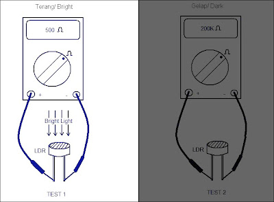
The resistance value of LDR (Light dependent resistor) will change with light intensity about it or around it. In dark conditions the resistance of approximately 200KΩ and LDR in bright Around 500Ω. LDR is made from semiconductor materials such as cadmium sulfide. With this material the energy of the light that falls cause more load to the electric current is released or increased. This means that the material resistance has decreased.

LDR can be easily tested by using a multimeter. because the resistance of an LDR varies according to the light falling on it. At bright light, the LDR resistance will be around 500Ohms and at darkness the resistance will be around 200K. For a proper diagnosis we need to measure the resistance of the LDR at bright light and at darkness.

Menguji LDR Gambar Cara Menguji LDR menggunakan Multi Meter

When exposed to light

Keep the multimeter at Ohms mode. The LDR must be subjected to a bright light source (day light is enough).Connect the LDR leads to the multimeter terminals as shown in the figure. Now the multimeter will show a low resistance reading around 500 Ohms.

When dark

Keep the multimeter at Ohms mode. The LDR must be subjected to darkness by covering it with an opaque paper. Connect the LDR leads to the multimeter terminals as shown in the figure. Now the multimeter will show a high resistance reading around 200K.

READMORE...

Rangkaian Pre- Amp mic 3 input - lm741

This is a 3 input mic mixer circuit using IC LM 741. Four 741s are used here. IC1, IC2, IC3 are used as preamplifiers. They produce a gain of around 40 decibel to the individual input signals. IC4 is wired as a summing amplifier to add the signals from three preamplifiers.IC4 also gives a gain of around 5 decibel to the final output signal. Total gain of the system is around 45 decibel.

Pre- Amp mic 3 inputSkema Rangkaian Pre- Amp mic 3 input


Note:
• Use+15/-15 V DC dual power for powering this circuit.
• All inputs and output must be connected with respect to the ground.
• Capacitors C1, C2 and C3 must be rated 10V and other capacitors must be 30V.


General Description

IC LM 741
Lay out IC LM 741

The LM741 series are general purpose operational amplifiers which feature improved performance over industry standards like the LM709. They are direct, plug-in replacements for the 709C, LM201, MC1439 and 748 in most applications. The amplifiers offer many features which make their application nearly foolproof: overload protection on the input and output, no latch-up when the common mode range is exceeded, as well as freedom from oscillations. The LM741C is identical to the LM741/LM741A except that the LM741C has their performance guaranteed over a 0°C to +70°C temperature range, instead of −55°C to +125°C.

READMORE...

Pemancar Fm 88-108Mhz - IC MAX2606

This is a FM transmitter circuit using Maxim semiconductors IC MAX2606. In the circuit the nominal frequency is set to 100 Mhz by inductor L1, (390nH) . The left and right channel audio signals from your source are added by R3 and R4, and attenuated by the POT R2. R2 can be used as a volume control .POT R1 can be used to select a channel of transmission between 88Mhz and 108Mhz.Use 80 cm long wire as the antena.

Pemancar Fm 88-108MhzSkema Rangkaian Pemancar Fm 88-108Mhz


Note:
* Use a battery for powering the circuit.It will reduce noise.
* An FM antenna from a old radio is a better option than the wire antenna.


IC MAX2606 Description

The MAX2605-MAX2609 are compact, high-performance intermediate-frequency (IF) voltage-controlled oscillators (VCOs) designed specifically for demanding portable wireless communication systems. They combine monolithic construction with low-noise, low-power operation in a tiny 6-pin SOT23 package.

These low-noise VCOs feature an on-chip varactor and feedback capacitors that eliminate the need for external tuning elements, making the MAX2605-MAX2609 ideal for portable systems. Only an external inductor is required to set the oscillation frequency. In addition, an integrated differential output buffer is provided for driving a mixer or prescaler. The buffer output is capable of supplying up to -8dBm (differential) with a simple power match. It also provides isolation from load impedance variations.

The MAX2605-MAX2609 operate from a single +2.7V to +5.5V supply and offer low current consumption. These IF oscillators can cover the 45MHz to 650MHz frequency range.

Pin IC MAX2606
IC MAX2606 Absolute Maximum Rating
  • VCC to GND..............................................................-0.3V to +6V
  • IND to GND ................................................-0.6V to (VCC + 0.3V)
  • TUNE to GND .............................................-0.3V to (VCC + 0.3V)
  • OUT+, OUT- to GND ..................................-0.3V to (VCC + 0.6V)
  • Continuous Power Dissipation (TA = +85°C)
  • 6-Pin SOT23 (derate 8.7mW/°C above +70°C)...........696mW
  • Operating Temperature Range ...........................-40°C to +85°C
  • Junction Temperature......................................................+150°C
  • Storage Temperature Range .............................-65°C to +150°C
  • Lead Temperature (soldering, 10s) .................................+300°C

READMORE...

Tuesday, September 15, 2009

Rangkaian 3 band Graphic Equalizer

This is the circuitof 3 band graphic equalizer using IC LF351 and few components. IC LF351 which is a wide bandwidth single JFET operational amplifier. The high input impedance of the IC makes this circuit compatible with most of the audio signal sources. The opamp is wired as an inverting amplifier. The input signal is fed to the inverting input of the opamp via the filter network. The filter network can produce a +/- 20 dB enhancement or cut on the three frequency bands 50Hz,1KHz and 10KHz.POTs R1, R2 and R3 can be used for adjusting the gain of the different bands.
3 band Graphic Equalizer
Skema Rangkaian 3 band Graphic Equalizer

This Circuit can be powered from anything between 6 to 30V DC, increasing supply voltage will increase the gain and the electrolytic capacitors must be rated higher than the supply voltage.

Description IC LF351

The LF351 is JFET input operational amplifier with an internally compensated input offset voltage. The JFET input device provides wide bandwidth, low input bias currents and offset currents.

Lay out IC LF351

IC LF351
Features IC LF351
• Internally trimmed offset voltage: 10mV
• Low input bias current : 50pA
• Wide gain bandwidth : 4MHz
• High slew rate : 13V/μs
• High input impedance : 1012Ω

READMORE...

Sunday, September 13, 2009

Rangkaian Penguji Transistor

This is a circuit can b e used to check the hfe of transistors. Both PNP and NPN transistors can be checked using this circuit. Hfe as high as 1000 can be measured by using this circuit. This circuit is based on two constant current sources build around transistors Q1 and Q2. Q1 is a PNP transistor and the constant current flows in the emitter lead. The value of constant current can be given by the equation; (V D1 -0.6)/ (R2+R4).The POT R4 can be adjusted to get a constant current of 10uA.

Q2 is an NPN transistor and the constant current flows into the collector lead. The value of this constant current can be given by the equation; (VD2-0.6)/(R3+R5).The POT R5 can be adjusted to get a constant current of 10uA.This constant current provided by the Q1 circuit if the transistor under test is an NPN transistor and by Q2 circuit if the transistor under test is a PNP transistor is fed to the base of transistor under test. This current multiplied by the hfe flows in the collector of the transistor and it will be indicated by the meter. The meter can be directly calibrated to read the hfe of the transistor.
Penguji TransistorSkema Rangkaian Penguji Transistor

List Component
  • D1,D2: Diode Zener 5.6volt 1/2 watt
  • Q1: 2N2907 PNP transistor
  • Q2: 2N222 NPN transistor
  • R2,R3: 470K Resistor
  • R4,R5: 100K Variable Resistot (Potensiometer)
  • M1: Miliampere meter Analog (10mA)
  • J1,J2: transistor sockets

READMORE...

Lampu otomatis menggunakan photocell (LDR)

This is a photocell circuit for detecting the light intensity. At full light the resistance of the photocell will be few ten ohms and at darkness it will rise to several hundred ohms. IC1 Op amp uA741 is wired as a comparator here. At darkness the resistance of photocell increases and so the voltage at the inverting input of the IC1 will be less than the reference voltage at the non inverting input. The output of the IC1 goes to positive saturation and it switches ON the transistor to activate the relay. By this way the lamp connected through the relay contact glows. The diode D1 works as a freewheeling diode.

Lampu otomatis
Rangkaian Lampu otomatis menggunakan photocell (LDR)


photocell


A light sensor (photodetector) that varies its resistance between its two terminals based on the amount of photons (light) it receives. Used for photographic light meters, automatic on-at-dusk street lights and other light-sensitive applications, it is also called a "light dependent resistor" (LDR) and "photoresistor."

The photocell's semiconductor material is typically cadmium sulfide (CdS), but other elements are also used. Photocells and photodiodes are used for similar applications; however, the photocell passes current bi-directionally, whereas the photodiode is unidirectional.

photocell
Gambar photocell

Photocells come in a variety of packages such as this assortment from PerkinElmer. As the photocell receives more photons, the resistance is lowered between the two terminals.

READMORE...

Karakteristik Tegangan Dioda Zener

dioda zener
Gambar dan simbol dioda zener

Zener diode is specially designed to operate in the reverse biased mode. It is acting as normal diode while forward biasing. It has a particular voltage known as break down voltage, at which the diode break downs while reverse biased. In the case of normal diodes the diode damages at the break down voltage. But zener diode is specially designed to operate in the reverse breakdown region.

The principle of zener diode is the zener breakdown. When a diode is heavily doped, it’s depletion region will be narrow. When a high reverse voltage is applied across the junction, there will be very strong electric field at the junction. And the electron hole pair generation takes place. Thus heavy current flows. This is known as Zener break down.

So a zener diode, in a forward biased condition acts as a normal diode. In reverse biased mode, after the break down of junction current through diode increases sharply. But the voltage across it remains constant

Karakteristik Dioda zener
Gambar Karakteristik Tegangan Diode zener

Funsi dioda Zener

Zener function is to stabilize the voltage. At the time connected in parallel with a source voltage swings are installed so that the ration-back, a zener diode will act like a short circuit (short-circuit) voltage when the voltage reaches the diode damage. The result, the voltage will be limited to a number that has been known previously.

Aplikasi dioda zener

READMORE...

Friday, September 11, 2009

Rangkaian 100watt Inverter 2N3055

This is a 100 Watt inverter circuit using minimum number of components. Here circuit used IC CD 4047 IC from Texas Instruments for generating the 100 Hz pulses and four 2N3055 transistors for driving the load.

IC1 Cd4047 wired as an astable multivibrator produces two 180 degree out of phase 100 Hz pulse trains. These pulse trains are are preamplifes by the two TIP122 transistors. The out puts of the TIP 122 transistors are amplified by four 2N 3055 transistors (two transistors for each half cycle) to drive the inverter transformer. The 220V AC will be available at the secondary of the transformer.Nothing complex just the elementary inverter principle and the circuit works great for small loads like a few bulbs or fans.If you need just a low cost inverter in the region of 100 W,then this is the best.

Inverter 100watt

Skema Rangkaian Inverter 100watt 2N3055


The maximum allowed output power of an inverter depends on two factors.The maximum current rating of the transformer primary and the current rating of the driving transistors, For example ,to get a 100 Watt output using 12 V car battery the primary current will be ~8A ,(100/12) because P=VxI.So the primary of transformer must be rated above 8A. Also here ,each final driver transistors must be rated above 4A. Here two will be conducting parallel in each half cycle, so I=8/2 = 4A .


Note:

  • A 12 V car battery can be used as the 12V source.
  • Use the POT R1 to set the output frequency to50Hz.
  • For the transformer get a 9-0-9 V , 10A step down transformer.But here the 9-0-9 V winding will be the primary and 220V winding will be the secondary.

IC CD4047 Description


IC CD4047


IC CD4047B is capable of operating in either the monostable or astable mode. It requires an external capacitor (between pins 1 and 3) and an external resistor (between pins 2 and
3) to determine the output pulse width in the monostable mode, and the output frequency in the astable mode. Astable operation is enabled by a high level on the astable input or low level on the astable input. The output frequency (at 50% duty cycle) at Q and Q outputs is determined by the
timing components. A frequency twice that of Q is available at the Oscillator Output; a 50% duty cycle is not guaranteed. Monostable operation is obtained when the device is triggered
by low-to-high transition at a trigger input or high-tolow transition at b trigger input. The device can be retriggered by applying a simultaneous low-to-high transition to both the a trigger and retrigger inputs. A high level on Reset input resets the outputs Q to low, Q to
high.

READMORE...

Thursday, September 10, 2009

Control Kecapatan Fan-Metode PWM

The following circuit is a circuit that is used to adjust the fan speed by using the PWM (Pulse Width Modulation). This circuit is very easy to make, and do not use the microcontroller or other digital components, for more details, let's look at his series of pictures below

Control Kecapatan FanSkema Rangkain Control Kecapatan Fan-Metode PWM


VR1: 10K Potentiometer Function as the motor speed control.

R9: Resistor as a determinant of minimum speed. Diseri with 10K VR, R1 for 1K will provide the settings range from 0 - 100% better used if the load used is a motor or a lamp. If R1 for 10K, will provide the range 5V - 12V is suitable if the load used is the cooling fan.

Q1: For 600mA maximum load, we recommend using the 2N2222A transistors packed in a metal body (TO-18). To load up to 5A please try using a transistor TIP120, 121 or 122.

D1: Diode is used to prevent back-emf which usually occurs in the load inductor such as Fan or Motor. Back-emf can damage the transistor!


Lay out PCD pic
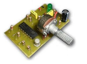
Finished Rangkaian Control Kecapatan Fan


Description IC The LM124 Low Power Quad Operational Amplifier

The LM124 series consists of four independent, high gain, internally frequency compensated operational amplifiers which were designed specifically to operate from a single power supply over a wide range of voltages. Operation from split power supplies is also possible and the low power supply current drain is independent of the magnitude of the power supply voltage.

Application areas include transducer amplifiers, DC gain blocks and all the conventional op amp circuits which now can be more easily implemented in single power supply systems. For example, the LM124 series can be directly operated off of the standard +5V power supply voltage which is used in digital systems and will easily provide the required interface electronics without requiring the additional ±15V power supplies.


READMORE...

Pengisi Battery Li-On Menggunakan USB

USB port it is one of the most useful port. Besides being used as an interface port for the device I / O computer, this port was also used as a filler Li-On Battery (Li-On Battery Charger). Battery charger circuit Li-On can you see in the image below


Pengisi BatterySkema Rangkaian Pengisi Battery Li-On

USB port capable of supplying a maximum voltage 5.25 V with a maximum flow of 0.5 A. Therefore, the above series can only be used to fill a Li-On Battery only. As LM3622 controller IC is used. IC's main function is as decisive end and a battery charging.


IC lm3622 Description

The LM3622 is a charge controller for Lithium-Ion batteries. This monolithic integrated circuit accurately controls an external pass transistor for precision Lithium-Ion battery charging. The LM3622 provides a constant voltage or constant current (CVCC) configuration that changes, as necessary, to optimally charge lithium-ion battery cells. Voltage charging versions (4.1V, 4.2V, 8.2V, and 8.4V) are available for one or two cell battery packs and for coke or graphite anode battery chemistry.

The LM3622 accepts input voltages from 4.5V to 24V. Controller accuracy over temperature is ±30mV/cell for A grade and ±50mV/cell for the standard grade. No precision external resistors are required. Furthermore, the LM3622's proprietary output voltage sensing circuit drains less than 200nA from the battery when the input source is disconnected.

The LM3622 circuitry includes functions for regulating the charge voltage with a temperature compensated bandgap reference and regulating the current with an external sense resistor. The internal bandgap insures excellent controller performance over the operating temperature and input supply range.

The LM3622 can sink 15mA minimum at the EXT pin to drive the base of an external PNP pass transistor. It also has low-voltage battery threshold circuitry that removes this drive when the cell voltage drops below a preset limit. The LVSEL pin programs this threshold voltage to either 2.7V/cell or 2.15V/cell. The low-voltage detection, which is a user enabled feature, provides an output signal that can be used to enable a "wake up charge" source automatically to precondition a deeply discharged pack.

Features IC lm3622
  • Versions for charging of 1 cell (4.1V or 4.2V) or 2 cells (8.2V or 8.4V)
  • Versions for coke or graphite anode
  • Precision (±30mV/cell) end-of-charge control
  • Wide input range: 4.5V-24V
  • Low battery drain leakage: 200nA
  • 15 mA available to drive low cost PNP

READMORE...

Sunday, September 06, 2009

Rangkaian Frekuensi Counter Digital

With a microcontroller system AT89c2051 and an LCD display we can create a digital frequency counter which can measure frequencies up to 250KHz. LCD is used LM16200.

LCD LM16200LM16200 LDC Pic
Table LM16200.Pin LCD LM16200

Scheme of frequency counter digital using AT89c2051 are as follows:
Frekuensi Counter DigitalSkema Rangkaian Frekuensi Counter Digutal

AT89c2051 to program, we use the Bascom 8051, the following programs Frequency caunter Digital Using AT89c2051:


'--------------------------------------------------------
' file: efy20fm24.BAS 25-12-05
' Frequency Meter Program using AT89c2051 micro controller
' written using bascom-51 from www.mcselec.com holland
' an embedded visual basic compiler for 8051 micro
' controllers
' by K.S.Sankar Web: www.mostek.biz
'------------------------------------------------------
' Connect the timer0 input P3.4 to a frequency generator
' with 24 mhz xtal accuracy ok upto 250khz
' define crystal speed and include file
$regfile = "89c2051.dat"
$crystal = 24000000
' define variables used
Dim A As Byte
Dim C As Long , D As Long
Dim Count As Word
Dim T0ic As Long
Dim Delayword As Word

' Initialize variables
Count = 0
T0ic = 0
D = 0
' initialize ports
P1 = 0
P3 = 255
' configure lcd display
Config Lcd = 16 * 2
Config Lcdpin = Pin , Db4 = P1.4 , Db5 = P1.5 , Db6 = P1.6 , Db7 = P1.7 , E = P1.3 , Rs = P1.2
Cls
'clear the LCD display
Lcd " EFY Freq Meter "
' define timer0
Config Timer0 = Counter , Gate = Internal , Mode = 1
'Timer0 = counter : timer0 operates as a counter
'Gate = Internal : no external gate control
'Mode = 1 : 16-bit counter
' set t0 internal interrupt
On Timer0 Timer_0_overflow_int
' interrupt will be generated on every 65536 count
Priority Set Timer0
Enable Interrupts
Enable Timer0

Counter0 = 0
'clear counter
Start Counter0
'enable the counter to count
Do
'set up a 1 sec accurate DO NOTHING loop
Enable Interrupts
'wait 1 as per BASCOM-51 is not accurate
For Delayword = 1 To 45440
Next Delayword
Disable Interrupts
C = Counter0
'get counter value
D = T0ic * 65536
Lowerline
C = C + D
T0ic = 0
Lcd " "
Lowerline
' show the frequency
Lcd "f=" ; C ; " Hz"
Waitms 255
Waitms 255
C = 0
Counter0 = 0
Start Counter0
're-start it because it was stopped by accessing the COUNTER
Loop

' timer0 int subroutine
Timer_0_overflow_int:
Rem timer0 overflow ( 65535 ) interrupt comes here
' increment the variable
Incr T0ic
Return
End
' end of program
' uses 1106 bytes of program memory

READMORE...

Rangkaian Microphone/Mic FM Wireless

Microphone/Mic FM Wireless is basically an FM transmitter to low power. FM Wireless Mic circuit you can use it to replace the wireless mic is usually quite expensive price. If you are a fan of electronics, then the series is worth your trying, but its component prices cheaper tool is also very useful. Here is a picture of his series:
Microphone/Mic FM  Wireless Skema Rangkaian Microphone/Mic FM Wireless


List Component of Microphone/Mic Wireless

1 = 10K (brown-black-orange)
R2,R3 = 100K (brown-black-yellow)
R4 = 470 ohm (yellow-violet-brown)
C1,C3 = 4.7pF (4p7), ceramic
C2,C4 = 4.7uF-16V, electrolytic
C5 = 0.001uF (1nF), ceramic
C6 = 470pF, ceramic
Q1,Q2 = 2N2222, NPN transistor
L1 = 1uH, variable inductor
Mic = Electret mike, 2 wires


Q1 amplifies the input signal via C4 from the electret microphone. Q2 acts as an oscillator and the signal coming off C2 is fed onto the base of Q2. L1/C1 is a so called ‘tank’ circuit and operates in the 88-105MHz band on your regular AM/FM radio dial.
L1 is a 1uH variable inductor coil to be able to tune it a little bit, and the range of 1uH is approximate. The antenna can be as simple as a 8″ (21cm) piece of wire of any kind.

READMORE...

Rangkaian Driver/Buffer Saklar Relay

This is a circuit instead of a standard on-off switch. Switching (Saklar) is very gentle. If we don’t use the PCB, connect unused input pins to an appropriate logic level (’+’ or ‘-’). Unused output pins *NEED* be left open!. One step ’push’ activates the relay, another ‘push’ de-activates the relay.


Driver/Buffer  Saklar Relay

Rangkaian Driver/Buffer Saklar Relay pIc


list Component Of Rangkaian Driver/Buffer Saklar Relay
R1 = 10K
R2 = 100K
R3 = 10K
R4 = 220 Ohm (optional)
C1 = 0.1µF, Ceramic (100nF)
C2 = 1µF/16V, Electrolytic
D1 = 1N4001
Led1 = Led, 3mm, red (optional)
Q1 = 2N4401 (see text) IC1 = 4069, CMOS, Hex Inverter (MC14069UB), or equivalent
S1 = Momentary on-switch
Ry1 = Relay

Description

This circuit operate on voltages from 3 to 18 volts, but most applications are in the 5-15 volts. Although the IC1 4069 contains protection circuitry against damage from ESD , use common sense when handling this device. Depending on your application you may want to use an IC-socket with IC1. It makes replacement easy if the IC ever fails. The IC is CMOS so watch for static discharge! You can use any type of 1/4 watt resistors including the metal-film type.

The type for D1 in not critical, even a 1N4148 will work. But, depending on your application I would suggest a 1N4001 as a minimum if your relay type is 0.5A or more. Any one in the 1N400x series diodes will work.

Any proper replacement for Q1 will work, including the european TUN’s. Since Q1 is just a driver to switch the relay coil, almost any type for the transistor will do. PN100, NTE123AP, BC547, 2N3904, 2N2222, 2N4013, etc. will all work for the relays mentioned here. For heavier relays you may need to change Q1 for the appropriate type.

For C2, if you find the relay acts not fast enough, you can change it to a lower value. It is there as a spark-arrestor together with diode D1.

For the relay I used an 8 volt type with the above circuit and a 9 volt battery. Depending on your application, if the current-draw is little, you can use a cheap 5V reed-relay type. Use a 8V or 9V relay type if your supply voltage is 12V. Or re-calculate resistor R3 for a higher value.

The circuit and 9V will work fine and will pull the relay between 7 and 9 volt, the only thing to watch for is the working voltage of C2; increase that to 50V if you use a 12V supply.

The pcb was designed for an Aromat/Omron relay, 12V/5A, #HB1-DC12V. You can easily re-design the relay pads on the PCB for the relay of your choice. If you wish to use something you already have, and you don’t want to re-design the PCB, you can glue the relay up-side-down on the pcb and wire the relay contacts manually to the pcb-holes or directly to your application. Use a 2N2222 transistor for Q1 if your supply voltage is higher than 9V and/or your relay is heavy duty, or doesn’t want to pull-in for any other reason.

Again, the pcb drawing is not to scale. Use ‘page-setup’ to put the scale to 103% for a single pcb, vertically, and your scale should be correct. I use a laser printer and so I don’t know if this scale of 103% is for all printers. To check, print a copy onto regular paper and see if the IC pins fit the print. If so, your copy is correct. If not, change the scale up of down until a hardcopy fits the IC perfectly.

The Led is nice for a visual circuit indication of being ‘on’. For use with 12V supply try making make R4 about 330 ohms. The LED and R4 are of course optional and can be omitted. Your application may already have some sort of indicator and so the LED and R4 are not needed.

READMORE...
 
Skema Rangkaian Elektronika