Showing posts with label Timer/ Osilator. Show all posts

Friday, February 11, 2011

Triangle and Squarewave Generator Using Op-Amp

Triangle and Squarewave Generator CircuitThe circuit shows a simple triangle and squarewave generator using a common LM1558 dual op-amp to produce very low frequencies to about 10 KHz. The time interval for one half cycle is about R*C and the outputs will supply about 10mA. Triangle amplitude can be altered by adjusting the 47k resistor and waveform offset can be removed by adding a capacitor in series with the output.

LM1558 Pin-out
Absolute Maximum Ratings Of Op-Amp LM1558 IC
  • Supply Voltage ±22V
  • Power Dissipation 400 mW
  • Differential Input Voltage ±30V
  • Input Voltage (Note 3) ±15V
  • Operating Temperature Range −55°C to +125°C
  • Storage Temperature Range −65°C to +150°C
  • Lead Temperature (Soldering, 10 sec.) 260°C

READMORE...

Monday, January 10, 2011

Rangkaian 8038 frequency | Signal Generator

frequency | Signal Generator circuit is a circuit that produces a variety of different waveforms at a desired frequency. It can generate Sine waves, Square waves, Triangular and Sawtooth waveforms as well as other types of output waveforms. There are many "off-the-shelf" waveform generator IC's available and all can be incorporated into a circuit to produce the different periodic waveforms.

Rangkaian 8038 frequency | Signal Generator Skema Rangkaian 8038 frequency | Signal Generator

IC 8038 Pinout IC 8038 Pinout

One such device is the 8038 a precision waveform generator IC capable of producing sine, square and triangular output waveforms, with a minimum number of external components or adjustments. Its operating frequency range can be selected over eight decades of frequency, from 0.001Hz to 300kHz, by the correct choice of the external R-C components.

The frequency of oscillation is highly stable over a wide range of temperature and supply voltage changes and frequencies as high as 1MHz is possible. Each of the three basic waveform outputs, sine, triangle and square are simultaneously available from independent output terminals. The frequency range of the 8038 is voltage controllable but not a linear function. The triangle symmetry and hence the sine wave distortion are adjustable.

READMORE...

Sunday, January 09, 2011

Bistable Multivibrator Using IC 555 Circuit

555 Bistable Multivibrator circuit acts as a basic flip-flop. The Output will stable in two states: output high and output low. The switching of the output waveform is achieved by controlling the Trigger and Reset inputs which are held "HIGH" by the two pull-up resistors, R1 and R2. By taking the Trigger input (pin 2) "LOW", switch in Set position, changes the output state into the "HIGH" state and by taking the Reset input (pin 4) "LOW", switch in Reset position, changes the output into the "LOW" state. This 555 timer circuit will remain in either state indefinitely and is therefore bistable. Then the Bistable 555 timer is stable in both states, "HIGH" and "LOW".

555 Bistable Timer CircuitSkema Rangkaian 555 Bistable Multivibrator


Note:
  • Trigger (555 pin 2) makes the output high, Trigger is 'active low', it functions when <>
  • Reset (555 pin 4) makes the output low. Reset is 'active low', it resets when <>
  • The power-on reset, power-on trigger and edge-triggering circuits can all be used as described above for the

READMORE...

Saturday, January 08, 2011

IC 555 Monostable Circuit

Monostable circuit produces one pulse of a set length in response to a trigger input Such as a push button. The output of the circuit stays in the low state Until there is a trigger input, Hence the name "monostable" meaning "one stable state".

This type of circuit is ideal for use in a "push to operate" system for a model displayed at EXHIBITIONS. A visitor cans push a button to start a model's mechanism, moving, and the mechanism will from automatically switches off after a set time.

The circuit diagram of the 555 monostable circuit is given as follows.

Monostable Using IC 555 Circuit Monostable Using IC 555 Circuit

IC 555 Pinout

Note:
  • resistor value R and the capacitor value C are unspecified. The values of these components determine the length of time that the monostable output is in the high state, and they may be calculated using the equation below
  • T = 1.1RC or R = T/1.1C

In the monostable mode, the timer 555 acts as a "one-shot" pulse generator. The pulse Begins Pls the 555 timer receives a signal at the trigger input That falls below a third of the voltage supply. The width of the output pulse is determined by the time constant of an RC network, the which consists of a capacitor (C) and a resistor (R). The output pulse ends Pls the charge on the C equals 2 / 3 of the supply voltage. The output pulse width cans be lengthened or shortened to the need of the specific application by adjusting the values of R and C

READMORE...

Tuesday, December 28, 2010

Simple switch-Off Time Delay Circuit

Designing a switch off delay circuit is quite simple and will cost you no more than $5 to make. All parts can be picked up from Radio Shack or Fry's if you have them as well as Parts Express. This will cover the mechanical aspects of it - theoretical topics can come later. If you suffer from pops on your amps or any other components, this will help you eliminate it, but it does not work in all cases.

Simple switch-Off Time Delay CircuitSimple switch-Off Time Delay Circuit

Designing a swictch off delay circuit is quite simple and will cost you no more than $5 to make. All parts can be picked up from Radio Shack or Fry's if you have them as well as Parts Express. This will cover the mechanical aspects of it - theoretical topics can come later. If you suffer from pops on your amps or any other components, this will help you eliminate it, but it does not work in all cases.

The two circuits di atas illustrate opening a relay contact a short time after the ignition or ligh switch is turned off. The capacitor is charged and the relay is closed when the voltage at the diode anode rises to 12 volts. The circuit on the left is a common collector or emitter follower and has the advantage of one less part since a resistor is not needed in series with the transistor base. However the voltage across the relay coil will be two diode drops less than the supply voltage, or about 11 volts for a 12.5 volt input. The common emitter configuration on the right offers the advantage of the full supply voltage across the load for most of the delay time, which makes the relay pull-in and drop-out voltages less of a concern but requires an extra resistor in series with transistor base. The common emitter (circuit on the right) is the better circuit since the series base resistor can be selected to obtain the desired delay time whereas the capacitor must be selected for the common collector (or an additional resistor used in parallel with the capacitor).

The time delay for the common emitter will be approximately 3 time constants or 3*R*C. The capacitor/resistor values can be worked out from the relay coil current and transistor gain. For example a 120 ohm relay coil will draw 100 mA at 12 volts and assumming a transistor gain of 30, the base current will be 100/30 = 3 mA. The voltage across the resistor will be the supply voltage minus two diode drops or 12-1.4 = 10.6. The resistor value will be the voltage/current = 10.6/0.003 = 3533 or about 3.6K. The capacitor value for a 15 second delay will be 15/3R = 1327 uF. We can use a standard 1000 uF capacitor and increase the resistor proportionally to get 15 seconds.

Source: bowdenshobbycircuits.info

READMORE...

Monday, December 27, 2010

Simple Switch On Time Delay Circuit

This Switch On Time Delay circuit has been designed to create a lamp switch operated electronically with an option of setting a delay in the time of execution of operation to reduce one or more lamps in a stairwell or any other places where this circuit may be useful. The circuit can be useful to control various lamp or appliances that can be connected in relay contacts.

Switch On Time Delay  CircuitSimple Switch On Time Delay Circuit

The circuit that takes advantage of the emitter/base breakdown voltage of an ordinary bi-polar transistor. The reverse connected emitter/base junction of a 2N3904 transistor is used as an 8 volt zener diode which creates a higher turn-on voltage for the Darlington connected transistor pair. Most any bi-polar transistor may be used, but the zener voltage will vary from about 6 to 9 volts depending on the particular transistor used. Time delay is roughly 7 seconds using a 47K resistor and 100uF capacitor and can be reduced by reducing the R or C values. Longer delays can be obtained with a larger capacitor, the timing resistor probably shouldn't be increased past 47K. This Switch On Time Delay circuit should work with most any 12 volt DC relay that has a coil resistance of 75 ohms or more. The 10K resistor connected across the supply provides a discharge path for the capacitor when power is turned off and is not needed if the power supply already has a bleeder resistor.

Sumber: http://www.bowdenshobbycircuits.info

READMORE...

9 Second Countdown Power-On Relay With 7 segment Display

9 Second Countdown Power-On Relay Circuit 9 Second Countdown Power-On Relay Circuit

This circuit provides a 9 second delay using a 7 segment display. When the switch is closed, the CD4010 up/down counter is preset to 9 and the 555 timer is disabled with the output held high. When the switch is opened, the timer produces an approximate 1 second clock signal, decrementing the counter until the 0 count is reached. When the zero count is reached, the 'carry out' signal at pin 7 of the counter moves low, energizing the 12 volt relay and stopping the clock with a low signal on the reset line (pin 4). The relay will remain energized until the switch is again closed, resetting the counter to 9. The 1 second clock signal from the 555 timer can be adjusted slightly longer or shorter by increasing or decreasing the resistor value at pin 3 of the timer.

Note:
  • The circuit can be powered from a 9V PP3 battery or 12V DC power supply.
  • The time delay can be varied by replace the resistor value at pin 3 IC555.
  • The push button switch is for starting the timer.
  • The appliance can be connected via contacts relay.

Source: bowdenshobbycircuits.info

READMORE...

Wednesday, December 08, 2010

Rangkaian 50Hz Accurate Oscillator

This circuit is a getting a 50Hz pulse. The oscillator circuit need only provide the IC ELM446, crystal and two appropriate loading capacitors
Rangkaian 50Hz Accurate OscillatorSkema Rangkaian 50Hz Accurate Oscillator
Note:
  • for greater accuracy as usual, it is also good practice to place a bypass capacitor across the power supply as well

The IC ELM446 is an 8 pin digital divider integrated circuit, that provides both 50Hz and 1Hz outputs from a common 3.58MHz NTSC colourburst crystal. Externally, the designer need only provide the crystal and two appropriate loading capacitors, as well as a suitably bypassed power supply. Internal Oscillator circuits then use this reference frequency to precisely derive a stable 50Hz signal. For convenience, a complementary 50Hz signal is also provided. This signal is then further divided to provide a 1Hz signal output. By ELM Electronics
IC ELM446This is pinout of IC ELM446, If you need more detail please download ELM446's pdf datasheet.

READMORE...

Sunday, November 28, 2010

Rangkaian On/Off 24 Hours Timer

This is a circuits are multi-range timers offering periods of up to 24 hours and beyond. This circuit can be used as repeating timers - or as single-shot timers

Rangkaian On/Off 24 Hours TimerSkema Rangkaian On/Off 24 Hours Timer

The Cmos 4060 is a 14-bit binary counter. However - only ten of those bits are connected to output pins. The 4060 also has two inverters - connected in series across pins 11, 10 & 9. Together with R3, R4, R5 and C3 - they form a simple oscillator.

While the oscillator is running - the 14-bit counter counts the number of oscillations - and the state of the count is reflected in the output pins. By adjusting R4 you can alter the frequency of the oscillator. So you can control the speed at which the count progresses. In other words - you can decide how long it will take for any given output pin to go high.

When that pin goes high - it switches the transistor - and the transistor in turn operates the relay. In single-shot mode - the output pin does a second job. It uses D1 to disable the oscillator - so the count stops with the output pin high.

If you want to use the timer in repeating mode - simply leave out D1. The count will carry on indefinitely. And the output pin will continue to switch the transistor on and off - at the same regular time intervals.

Note:
  • Using "Trial and Error" to set a long time period would be very tedious. A better solution is to use the Setup tables provided - and calculate the time required for Pin 7 to go high. For example, if you want a period of 9 Hours - the Range table shows that you can use the output at Pin 2. You need Pin 2 to go high after 9 x 60 x 60 = 32 400 seconds. The Setup table tells you to divide this by 512 - giving about 63 seconds. Adjust R4 so that the Yellow LED lights 63 seconds after power is applied. This will give an output at Pin 2 after about 9 Hours.
  • Ideally C3 should be non-polarized - but a regular electrolytic will work - provided it doesn't leak too badly in the reverse direction. Alternatively - you can simulate a non-polarized 10uF capacitor by connecting two 22uF capacitors back to back
  • The timers were designed for a 12-volt supply. However - provided a suitable relay is used - both circuits will work at anything from 5 to 15-volts. Applying power starts the timer. And it can be reset at any time by a brief interruption of the power supply.
Sorcer: http://www.zen22142.zen.co.uk/

READMORE...

Wednesday, September 01, 2010

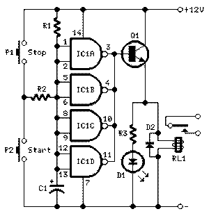
Rangkaian ON OFF Sleep Timer Switch

ON/OFF Sleep Timer Switch

This timer was designed mainly to switch off a portable radio after some time: in this way, one can fall asleep on the sand or on a hammock, resting assured that the receiver will switch off automatically after some time, saving battery costs.

Rangkaian ON OFF Sleep Timer SwitchSkema Rangkaian ON OFF Sleep Timer Switch

R1 and C1 provide a very long time constant. When P2 is momentarily closed, C1 discharges and the near zero voltage at its positive lead is applied to the high impedance inputs of the four gates of IC1 wired in parallel. The four paralleled gate outputs of the IC go therefore to the high state and the battery voltage is available at Q1 Emitter. When P2 is released, C1 starts charging slowly through R1 and when the voltage at its positive lead has reached about half the battery voltage, the IC gate outputs fall to zero, stopping Q1. This transistor can directly drive a portable radio receiver or different devices drawing a current up to about 250mA. Connecting a Relay across the Emitter of Q1 and negative ground, devices requiring much higher voltage and current operation can be driven through its contacts.

Pushing on P2 for 1 to 5 seconds, the circuit starts and then will switch off after about 35 minutes. This time delay can be varied by changing R1 and/or C1 values. P1 will stop the timer if required. LED D1 is optional and can be useful to signal relay operation when the load is placed far from the timer.

List Component
  • R1: 10M 1/4W Resistor
  • R2: 4K7 1/4W Resistor
  • R3: 1K 1/4W Resistor
  • C1: 220µF/ 25V Electrolytic capacitor
  • D1: LED
  • D2: 1N4148
  • IC1: 4011 Quad 2 Input NAND Gate CMos IC
  • Q1: BC337
  • P1,P2: SPST Pushbuttons
  • RL1: 12V Relay
Source

READMORE...

Friday, January 22, 2010

Rangkaian Osilator Gelombang Sinus Variabel.

Osilator Gelombang Sinus Variabel (15 to 150kHz)

This is a circuit of sine wave oscillators covering a frequency range of 15 to 150kHz in four switched steps. Two conditions exist for a sinusoidal oscillator. Regenerative or positive feedback, and a closed loop gain of unity. The losses in the wien feedback circuit, are such that the open-loop gain of the amplifier must also exceed 3.

rangkaian osilator sinus variabelSkema rangkaian osilator sinus variabel


The circuit gain is provided by a FET type op-amp (LF351), but LF351 may be difficult to obtain, for a replacement you can use TL071CN or TL081CN. The Maplin order codes are RA67X and RA70M respectively. The wien network is a parallel combination of resistors and capacitors, in series with a series RC network. Regenerative feedback is applied from the op-amp output, to the serail RC input and continues. Stabilization is required to prevent the otherwise Uncontrolled oscillation from building up and becoming unstable.

There are two common methods of stabilizing a wien oscillator type. A thermistor with a NTC in the series leg of the feedback loop or an incandescent lamp (with a positive temperature coefficient) in the shunt leg of the feedback loop. The bulb used here is a 6V 60mA type Maplin code BT99H. A 12 Volt bulb rated 60mA or 40mA will also work. The feedback arrangement works as follows. As a bulb filament heats up its resistance increases. This will decrease the overall gain of the amplifier, as the output signal is fed back to the input.Similarly, if the output of the signal amplitude decreased Appearing at the bulb would be less, its filament resistance would drop and the gain would be increased. Therefore a stable output amplitude is produced. The 1k preset is adjusted for minimum distortion. Note that split supplies are used and a ganged 10k Potentiometer controls with a 10:1 frequency range.

READMORE...

Tuesday, December 22, 2009

Rangkaian Osilator Berbasis Kristal

This is circuit for accurate time-base generation using the readily available 3.5795MHz crystal commonly used in telecommunication equipment. Crystal-based oscillator with divider IC chain or a similar circuit in the form of an ASIC is used for time-base generation. The 3.5795MHz crystal is used in conjunction with a CD4060-based crystal oscillator- cum-divider (IC1). The crystal frequency is divided by 512 by IC1, which is further divided by 7 by CD4017 (IC2). IC2 is reset as soon as its Q7 output goes high.

rangkaian osilator berbasis kristalSkema rangkaian osilator berbasis kristal


Thus the crystal frequency is divided by 3584, giving the final output frequency of around 998.8 Hz. This frequency can be trimmed to exactly 1 kHz with the help of trimmer capacitor VC1 as shown in the figure. The 1kHz signal can be further divided using decade counters to generate the required time period. EFY lab note. To generate required gate for use in a frequency counter circuit, the final oscillator output needs to be followed by a toggle flip-flop. For example, a 1kHz clock, when applied to a toggle flip-flop will generate gates with 1-sec ‘on’ period and 1-sec ‘off’ period. This circuit is estimated to cost below Rs 50.

READMORE...

Sunday, November 08, 2009

Multivibrator Astable Menggunakan IC 555

Multivibrator is an electronic circuit that at a certain time only one of two output voltage levels, except during the transition period. The transition (switching) between the two levels of output voltage occurs quickly. Two state level of the multivibrator output voltage, which is stable and Quasistable.

Astable multivibrator is called when the output voltage levels generated by the multivibrator circuit is quasistable. The circuit will only change the state of the output voltage level between the 2 conditions, each state has a fixed period. Multivibrator circuit will work independently and no longer need a trigger. Period of time each output voltage level is determined by the components making up the circuit.

multivibrator astable used IC 555Skema rangkaian multivibrator astable used IC 555


The picture above is the astable multivibrator circuit. This circuit will work when the voltage applied to Vcc ration and ground her. This circuit has two conditions are always changing with time. Because changing the type is known as astable multivibrator. With constant changes of 0 and 1, then the multivibrator is also called a bistable multivibrator (multivibrator which has two stable state of 0 and 1).


This change in cycle length can be calculated using the following equation:

Period = t1 + t2
t1 = 0.7 x (RA + RB) XC
t2 = 0.7 xRBxC.
.

READMORE...

Saturday, November 07, 2009

Rangkaian Multivibrator Monostable IC 555

Rangkaian Multivibrator Monostable IC 555 is a pulse generator circuit in which the duration of the pulse is determined by the R-C connected to IC 555 timer. In such a vibrator, one state of output is stable while the other is quasi-stable (unstable). For auto-triggering of output from quasi-stable state to stable state energy is stored by an externally connected capaci tor C to a reference level. The time taken in storage determines the pulse width. The transition of output from stable state to quasi-stable state is accom­plished by external triggering.


multivibrator monostable

Skema rangkaian multivibrator monostable IC 555


Capacitor C has to charge through resistance RA. The larger the time constant RAC, the longer it takes for the capacitor voltage to reach +2/3VCC. In other words, the RC time constant controls the width of the output pulse. The time during which the timer output remains high is given as

tp = 1.0986 RAC
where RA is in ohms and C is in farads. The above relation is derived as below. Voltage across the capacitor at any instant during charging period is given as


vc = VCC (1- e-t/RAC)
Substituting vc = 2/3 VCC in above equation we get the time taken by the capacitor to charge from 0 to +2/3VCC.

So +2/3VCC. = VCC. (1 – e-t/RAC) or t – RAC loge 3 = 1.0986 RAC
So pulse width, tP = 1.0986 RAC s 1.1 RAC
The pulse width of the circuit may range from micro-seconds to many seconds. This circuit is widely used in industry for many different timing applications.
.

READMORE...

Tuesday, September 22, 2009

Osilator Gelomabang Kotak varibel 1Hz-10Khz

This is a Circuit of square wave generator using IC uA741. The circuit uses positive feedback for Schmitt trigger action and negative feedback for timing of the wave form.


Let us presume that the output is high and the capacitor C1 is fully discharged.C1 now starts charging via R2 and R1. When the voltage across C1 rises above that the Junction of R3 & R4,the output quickly switches to fully negative voltage.C1 now starts discharging and charges in the opposite direction.Again,when the negative voltage across C1 falls below that at pin 3,the circuit switches back quickly to the fully positive output value.The cycle repeats endlessly.

Osilator Gelomabang Kotak
Skema Rangkaian Osilator varibel 1Hz-10Khz

Note:
* The circuit has to be powered from a +9/-9 V DC dual power supply .
* The frequency of output can be varied by varying POT R1.
* The frequency range can be adjusted by changing the value of R3,R4 or C1.

IC UA741 DESCRIPTION

The UA741 is a high performance monolithic operational amplifier constructed on a single silicon chip. It is intented for a wide range of analog applications.
  • Summing amplifier
  • Voltage follower
  • Integrator
  • Active filter
  • Function generator
The high gain and wide range of operating voltages provide superior performances in integrator, summing amplifier and general feedback applications. The internal compensation network (6dB/ octave) insures stability in closed loop circuits.

lay out Ic UA741
Absolute maximum rating Ic UA741
  • Symbol Parameter UA741M UA741I UA741C Unit
  • Supply voltage (VCC) ±22 V
  • Differential Input Voltage (Vid ) ±30 V
  • Input Voltage (Vi ) ±15 V
  • Power Dissipation (Ptot) 500 mW
  • Storage Temperature Range (Tstg) -65 to +150 °C

READMORE...

Saturday, August 22, 2009

Rangkaian Variable frequency oscillator

555 timer IC provides practical solutions and relatively inexpensive for a variety of electronic applications related to the timing (timing). Especially two of the most popular application is a series of monostable and astable timing. The main components of this IC consists of comparators and flip-flop is realized with a lot of transistors.

The principle component of this type of work does not change but each manufacturer makes the IC design and technology different. Almost all manufacturers make this type of component, although with a different. For example National Semiconductor LM555 call it, Philips and Texas Instruments SE/NE555 call. Motorola / ON-Semi designed with CMOS transistors that power consumption was small enough and called it MC1455. Philips and Maxim make his version of the CMOS ICM7555 name. Although different names, but the function of each diagram and pin compatible with each other. It's just that there are several different specific characteristics such as power consumption, maximum frequency and so on.

Variable frequency oscillator
Variable frequency oscillatorSkema Rangkaian Variable frequency oscillator

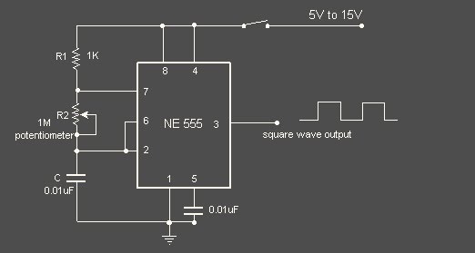
HereNE55 is wired as an astable multivibrator ,whose out put frequency can be varied by varying a potentiometer.This circuit is a must in the work bench of a electronic hobbyist.Frequencies ranging from several Hz to several KHz can be obtained using this circuit.For very low frequencies (few Hz) replace C with a higher value electrolytic capacitor.

The values of R and C can be obtained using the following equations.

1/f = 0.69 * C * ( R1 + 2*R2).

% duty cycle = 100*(R1+R2)/(R1+ 2*R2) .

The good option is to select R1 in K Ohms and R2 in M Ohms.


READMORE...

Friday, August 21, 2009

Rangkaian Ic 4060 Timer Dengan Alarm

The IC 4060 is a 14-stage ripple-carry binary counter/divider and oscillator with three oscillator terminals (RS, RTC and CTC), ten buffered outputs (O3 to O9 and O11 to O13) and an overriding asynchronous master reset input (MR). The oscillator configuration allows design of either RC or crystal oscillator circuits. The oscillator may be replaced by an external clock signal at input RS. The counter advances on the negative-going transition of RS.
A HIGH level on MR resets the counter (O3 to O9 and O11 to O13 = LOW), independent of other input conditions. Schmitt-trigger action in the clock input makes the circuit highly tolerant to slower clock rise and fall times.

Rangkaian Timer Dengan AlarmRangkaianIc 4060 Timer Dengan Alarm

A timer circuit using IC 4060 is given here. The IC 4060 is a 14 stage binary counter with a built-in oscillator.R2, R7, C1 are the components that determine the frequency of the oscillator and the outputs will become high one after other and only one at a time. The last five outputs are only used here. The high pulses from the outputs are used to trigger the NE555 IC. Here NE555 is wired as a monostable multivibrator. The buzzer will produce the alarm when the output of IC2 goes high. The duration of the alarm depends on the components C3 and R5.The duration can be adjusted by varying the value of C3.The alarm will automatically turn OFF after the predetermined time. The trigger pin of IC2 will be normally positive. When the Q1 is forward biased by the positive pulse at its base from IC1, the capacitor C2 becomes charged and reduces the voltage at trigger pin of IC2.This triggers the IC.When the capacitor is fully charged the pin 2 becomes again positive.
The maximum duration from timer IC 4060 will be at pin 3. The times decrease by half in the pins 2, 3, 15, and 13 respectively. The timer duration can be varied by varying the capacitor C1.

Notes
  • Use 6V DC for powering the circuit.
  • Mount the ICs on holders.
  • The switch S2 can be a single pole five throw rotary switch.
  • The switch S1 can be a push button switch.
  • S1 is used to reset the timer.
  • S2 is used to select the alarm time.
  • R7 can be used for the fine adjustment of alarm time.

READMORE...

Sunday, August 09, 2009

Rangkaian pembangkit Gelombang Terkontrol|variabel

Rangkaian pembangkit Gelombang Terkontrol|variabel

ICL8038 is a function generator chip, able of generating triangular, square , sine, pulse and sawtooth waveforms . From these sine, square & triangular wave forms can be made simultaneously. There is the option to control the parameters like frequency ,duty cycle and distortion of these functions. rangkian pembangkit gelombang ini is the best function generator circuit for a beginner to start with and is of course a must on the work bench of an electronics hobbyist. The circuit here is designed to produce waveforms from 20Hz to 2o kHz.The ICL 8038 has to be operated from a dual power supply.

Circuit Diagram & Parts List of Function Generator on show in the picture below.
Circuit of Function Generator Pembangkit Gelombang Sinus/kotak/segitiga dan Gigi gergaji

Notes .

  • frequency output can be adjusted using R7.It must be a 100K Log POT.
  • The duty cycle can be adjusted using R3 , a 1K POT.
  • Distortion owave form can be adjusted using R5 , a 100K POT.
  • Square,triangle & sine waveforms can be obtained simultaneously at pins 9,3,2 respectively.
Datasheet ICL 8038

The ICL8038 waveform generator is a monolithic integrated circuit capable of producing high accuracy sine, square, triangular, sawtooth and pulse waveforms with a minimum of external components. The frequency (or repetition rate) can be selected externally from 0.001Hz to more than 300kHz using either resistors or capacitors, and frequency modulation and sweeping can be accomplished with an external voltage. The ICL8038 is fabricated with advanced monolithic technology, using Schottky barrier diodes and thin film resistors, and the output is stable over a wide range of temperature and supply variations. These devices may be interfaced with phase locked loop circuitry to reduce temperature drift to less than 250ppm/oC.

Features ICL 8038
  • Low Frequency Drift with Temperature . . . . . 250ppm/oC
  • Low Distortion . . . . . . . . . . . . . . . 1% (Sine Wave Output)
  • High Linearity . . . . . . . . . . .0.1% (Triangle Wave Output)
  • Wide Frequency Range . . . . . . . . . . . .0.001Hz to 300kHz
  • Variable Duty Cycle . . . . . . . . . . . . . . . . . . . . . 2% to 98%
  • High Level Outputs. . . . . . . . . . . . . . . . . . . . . . TTL to 28V
  • Simultaneous Sine, Square, and Triangle WaveOutputs
  • Easy to Use - Just a Handful of External Components Required

READMORE...

Thursday, August 06, 2009

Pembangkit|Osilator gelombang sinus Wien bridge.

Pembangkit/osilator gelombang sinus is the main instrument that needs to exist in the electronics design of each workshop. For example, needed to test a series of audio HiFi requires sinusoidal signal as input.

Many circuits that can be used to generate a sine wave. And the most popular is the Clapp oscillator, oscillator Colpitt, crystal oscillator and Wien bridge. Each type has specific advantages and the implementation of each. Wien bridge oscillator is widely used in audio frequency mainly because of the frequency stability is good and relatively easy to make.

However, any posts at this time will be served in a series of sine wave oscillator (osilator gelombang sinus) Wien-bridge that can be realized with one op-amp and a few passive components.

Rangkaian osilator gelombang sinusSkema Rangkaian Pembangkit|Osilator gelombang sinus Wien bridge.

Rangkaian Pembangkit/osilator gelombang sinus will produce a series of sinusoidal waves with the frequency 1:59 kHz. But if you have tried this series and measure the results with osiloskop or frekuesi counter, the resonance frequency is 1.65 kHz. This is known because of the distortion in a series of sliding phasa the non-linier.

Compensation for the distortion, and can be used a series of nonlinear feedback. For example, replacing the resistor with a dc RG 6volt 1 watt, the large resistor RF should also be adjusted to more or less fixed value 2Rg. Large flow through the lamp will not light it, but enough to warm its filamen. Large resistansi lights change according to the heat because of the flow through it. This makes the op-amp is not a liner. In the series of the Wien bridge sine signal a more professional compensation is usually made by adding a set of AGC (automatic gain controller)

READMORE...

Friday, May 29, 2009

time delay with 555 chip


A time delay relay circuit is a relay that stays on for a certain amount of time once activated. This time delay relay is made up of a adjustable timer circuit which controls the actual relay. The time is adjustable from 0 to about 20 seconds with the parts specified. The current capacity of the circuit is only limited by what kind of relay you decide to use.

Note:
  • R1 adjusts the on delay time.
  • use a different capacitor for C1 to change the maximum on time.
  • S1 is used to activate the timing cycle.

READMORE...
 
Skema Rangkaian Elektronika