Sunday, August 30, 2009

Video Cara Mudah membuat PCB

How to make PCBs below my experience is the most practical, but the cost is very low, the result is no less attractive and neat compared to using the media Transfer Paper (original) the price quite expensive or printing etc that would be more complicated. Most of my friends probably already familiar with this method, but for others it never hurts to be used as an alternative.

Its very simple! watch the below video! What you all need is a circuit diagram, copper clads, sand papers, a printer, computer & an iron! You are done! I will explain the entire process later in words!


Video membuat PCB using Printer-leser

This video sows How to etch PCB using Ferric Chloride. You can do this in home in a simple way. Me too have done etching in home using Ferric Choride before & I am sure you will love this post.


Video membuat PCB using Ferric Chloride

READMORE...

Rangkaian Control Lampu Jalan Dengan LDR

This circuit is of a street light that automatically switches ON when the night falls and turns off when the sun rises. In fact you can this circuit for implementing any type of automatic night light. This circuit can be used to control lights or other electrical equipment with large power to hundreds of watts

The circuit used an LDR to sense the light . When there is light the resistance of LDR will be low. So the voltage drop across POT R2 will be high. This keeps the transistor Q1 ON. The collector of Q1(BC107) is coupled to base of Q2(SL100). So Q2 will be OFF and so do the relay. The bulb will remain OFF.

When night falls the resistance of LDR increases to make the voltage across the POT R2 to decrease below 0.6V. This makes transistor Q1 OFF which in turn turs ON Q2.The relay will be energized and the bulb will glow.

 Control Lampu Jalan Dengan LDRSkema rangkaian control lampu jalan dengan LDR

* POT R2 can be used to adjust the sensitivity of the circuit.
* You can use bulb of any wattage ,provided that relay should have the sufficient rating.
* The circuit can be powered from a regulated 9V DC power supply.
* Click Here! to get the power supply circuit for this project.
* The relay K1 can be a 9V SPDT relay.

A bout LDR ( Light Dependent Resistor )

Working principle of LDR is the LDR resistance will change with changes in light intensity about it. In the dark resistance of LDR about 10MΩ and in light of 1KΩ or less. LDR is made from semiconductor materials such as cadmium sulfide. With this material the energy of the light that falls cause more load to the electric current is released or increased. This means that the material resistance has decreased.
LDR ( Light Dependent Resistor )

LDR ( Light Dependent Resistor ) pic

LDR is used to convert light energy into electrical energy. Automatic light switches and burglar alarms are a few examples of tools that use the LDR. However, because the response to light is slow, LDR is not used in situations where the intensity of light changed drastically.

READMORE...

Saturday, August 29, 2009

Power Amplifier Sanken 1000 watt

This is a circuit of 1000watt power amplifier. This time I don't have a picture to the circuit board, but because the amplifier circuit is quite simple, you can design it yourself PCB easily or you can order it at the store PCB audio kit in the center of electronic singosaren oriental, solo.

amplifier 1000 watt
Skema Rangkaian Sanken 1000 watt

The assemble cables for DC power supply and output transistors must be large, use size 1.5-3mm for large current passed. The supply used transformer with 20A/45Ct and at least 4x10000uf/80 volt capasitor. this circuit is able to supply power 10000watt therefore the power transistor will be very hot, give good cooling fan on the power transisitor

Transitor alternative to replacement of the 2SA1494 is 2SA1216 From SANKEN. The transistor has a 200-350 watt power dissipation of each pair so that for long-term operation of more durable. Keep in mind, usually sold a pair of power transistors with its complement, so you can not buy 2SC2922 alone without 2SA1216 or 2SA1494 without 2SC3858. The price range for transitor tsb is 30-40 thousand Rupiah / pair.

READMORE...

Wednesday, August 26, 2009

Rangkaian Saklar sentuh Berbasis IC 555

Saklar sentuh Berbasis IC 555

This is the simple circuit of diagram of a small touch using IC NE 555 . This circuit is ideally useful for making touch operated doorbells, buzzers, toys etc which when touched on the touch plate operates the relay for a preset time and the turns off automatically.

the circuit is realized by utilizing the high input impedance of trigger pin of the IC 555. When the IC is triggered by the induced voltage of human body the output goes high for a time determined by R1 and C1. The transistor is used to drive the relay. The relay contacts can be used to drive the load like bell, motor , lights etc.

To setup the circuit connect to power supply and adjust R1 while keeping touching on the touch plate. Stop at the point where relay activates.If relay is in the activated state initially then do the same until the relay is deactivated.

Rangkaian Saklar sentuhSkema rangkaian saklar sentuh Berbasis IC 555

functions of each pin IC 555

https://blogger.googleusercontent.com/img/b/R29vZ2xl/AVvXsEiptMYXxB8qVVWyK2NmCReJSdCNrC4ZbEdb73MO64Sxua4pHzOFwtpjWfjdswUqDkBRt7XnZ6skfbNurVdNUa5ZjW98y7kscbvCy5IODG9CvuavLAjtEAdTxOvV0AZki45W29HWUZ1IsHY/s320/untitled.bmp

  1. Ground, is the input pin of the source of the negative DC voltage
  2. trigger, negative input from the lower comparators (comparator B) that maintain oscillation capacitor voltage in the lowest 1 / 3 Vcc and set RS flip-flop
  3. output, the output pin of the IC 555.
  4. reset, the pin that serves to reset the latch inside the IC to be influential to reset the IC work. This pin is connected to a PNP-type transistor gate, so the transistor will be active if given a logic low. Normally this pin is connected directly to Vcc to prevent reset
  5. control voltage, this pin serves to regulate the stability of the reference voltage negative input (comparator A). This pin can be left hanging, but to ensure the stability of the reference comparator A, usually associated with a capacitor of about 10nF to berorde pin groun
  6. threshold, this pin is connected to the positive input (comparator A) which will reset the RS flip-flop when the voltage on the capacitor from exceeding 2 / 3 Vc
  7. discharge, this pin is connected to an open collector transistor Q1 is connected to ground emitternya. Switching transistor serves to clamp the corresponding node to ground on the timing of certain
  8. vcc, pin it to receive a DC voltage supply. Usually will work optimally if given a 5-15V. the current supply can be seen in the datasheet, which is about 10-15mA.
.

READMORE...

Rangkaian Fan Control suhu otomatis

This circuit of automatic Control suhu is based on two transistors that can be used to control the speed of a 12 V DC fan depending on the temperature (suhu). A thermistor (R1) is used to sense the temperature. When the temperature increases the base current of Q1 (BC 547) increases which in turn decreases the collector voltage of the same transistor. Since the collector of Q1 is coupled to the base of Q2 (BD 140), the decrease in collector voltage of Q1 forward biases the Q2 more and so do the speed of the motor. Also, the brightness of the LED will be proportional to the speed of the motor.

 Control suhu otomatis
Skema rangkaian fan control suhu otomatis

Note:
  • R1 can be a 15K @ 20°C ,N.T.C thermistor.
  • M1: DC Fan 12V,700mA fan motor.
  • Capacitor C1 must be rated 25V.
  • The circuit can be powered from a 12V PP3 battery or 12V DC power supply.

About thermistor

The standard leaded thermistors are calibrated and tested at 20 °C to a tolerance of ± 5 % or ± 10 %; however, tighter tolerance, point matched thermistors are readily available as are special point match temperatures to fit your application. Since these thermistors have only one controlled point of reference (the point match temperature), the resistance at other
temperatures is given by the “Resistance vs. Temperature Conversion Tables” for the appropriate material curve. The resistance value at any temperature is the ratio factor times the resistance at 25 °C. The resistance vs. temperature conversion tables can
be found at: www.vishay.com/doc?33004 and www.vishay.com/doc?33011.

READMORE...

Rangkaian Termometer Digital

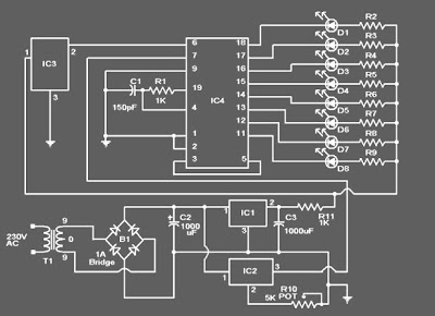
This circuit uses IC LM 35 to sense the temperature. output of LM 35 is given to the IC ADC 0804 (IC4) which converts the analog output of the LM 35 to digital output. The ADC 0804 is a 8 bit ADC .Eight LED’s are connected to the output of ADC to show the output logic.If needed the LED’s can be avoided and the output can be connected to any suitable external circuit like temperature controller etc.A 5V fixed voltage regulator based on 7805 (IC1) powers the circuit.Another variable voltage regulator based on LM317(IC2) is used to provide the reference voltage to the ADC 0804.

IC LM35Skema rangkaian termometer digital

Notes:
  • POT R10 can be used to adjust the scale factor of the ADC. The reference voltage at pin 7 of ADC0804 should be 2.5 V for full scale.
  • IC1: 7805, IC2: LM317, IC3: LM35, IC4 ADC0804
  • D1 TO D8: DIODE LED, R2 TO R8: 1K 1/2 WATT RESISTOR

Spesifikasi IC LM35

The LM35 series are precision integrated-circuit temperature sensors, whose output voltage is linearly proportional to the Celsius (Centigrade) temperature. The LM35 thus has an advantage over linear temperature sensors calibrated in ° Kelvin, as the user is not required to subtract a large constant voltage from its output to obtain convenient Centigrade scaling. The LM35 does not require any external calibration or trimming to provide typical accuracies of ±¼°C at room temperature and ±¾°C over a full -55 to +150°C temperature range. Low cost is assured by trimming and calibration at the wafer level. The LM35's low output impedance, linear output, and precise inherent calibration make interfacing to readout or control circuitry especially easy. It can be used with single power supplies, or with plus and minus supplies. As it draws only 60 µA from its supply, it has very low self-heating, less than 0.1°C in still air. The LM35 is rated to operate over a -55° to +150°C temperature range, while the LM35C is rated for a -40° to +110°C range (-10° with improved accuracy). The LM35 series is available packaged in hermetic TO-46 transistor packages, while the LM35C, LM35CA, and LM35D are also available in the plastic TO-92 transistor package. The LM35D is also available in an 8-lead surface mount small outline package and a plastic TO-220 package.


termometer digital

Feature IC LM35

•Calibrated directly in ° Celsius (Centigrade)
•Linear + 10.0 mV/°C scale factor
•0.5°C accuracy guaranteeable (at +25°C)
•Rated for full -55° to +150°C range
•Suitable for remote applications
•Low cost due to wafer-level trimming
•Operates from 4 to 30 volts
•Less than 60 µA current drain
•Low self-heating, 0.08°C in still air
•Nonlinearity only ±¼°C typical
•Low impedance output, 0.1 Ohm for 1 mA load

READMORE...

Rangkaian Monitor status battery 12 volt

This circuit can be used for monitoring the voltage level of an automobile battery. When battery voltage is 11.5V or less transistor Q1 will be On and LED D1 will be glowing.When battery voltage is between 11.5 - 13.5V, the transistor Q2 will be On and the LED D2 will be glowing.When battery voltage is above 13.5V the transistor Q3 will be On and the LED D3 will be glowing.

Monitor status battery 12 voltSkema rangkaian monitor status battery 12 volt

The battery 12 volt to be monitored can be connected between the terminals A and B and for convenience use LEDs of different colour .

List component of Monitor status battery 12 volt
-R1,R3,R6: 1k 1/4W Resistance
-R2: 100K 1/4W Resistance
-R4,R5,R7,R8: 3.3K 1/4W Resistance
-D1: LED red color
-D2: LED yellow color
-d7: LED green COLOR
-D2,D4,D5,D8,D9: 1N4148 diode 1 ampere
-D6: BZX79C10 diode Zener 10 volt
-D10: BZX79C12 diode Zener 12 volt
-Q1,Q2: BC547 NPN transistor
-Q3: BC557 PNP transistor

Spesifikasi BC547

This device is designed for use as general purpose amplifiers and switches requiring collector currents to 300 mA. Sourced from Process 10. See PN100A for characteristics.
Transistor BC547 (NPN General Purpose Amplifier)

Feature penting Transistor BC547
-(VCEO) Collector-Emitter: Voltage 45 V
-(VCES) Collector-Base Voltage: 50 V
-(VEBO) Emitter-Base Voltage: 6.0 V
-(IC) Collector Current: Continuous 500 mA
-(TJ) Tstg Operating and Storage Junction Temperature Range: -55 to +150 °C

READMORE...

Rangkaian Charging battery Mobil

This is a simple circuit that can be used for charging (mengisi) car battery. In this circuit there is facility for monitoring the charging current and voltage.


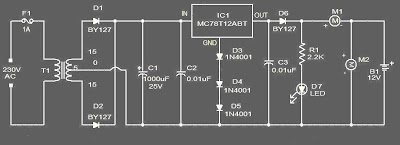
Circuit of charging battery Mobil is based on the IC MC78T12ABT . The IC is nothing but a 7812 in TO-3 package with 3A capacity. The transformer T1 steps the mains voltage to 15V AC and diodes D1&D2 does the job of rectification. Capacitor C1 does the filtering and C2 acts as a decoupling capacitor. The ground terminal of IC1 is lifted to 2.1V using the diodes D3 , D4 and D5 . So the output from the IC1 will be a regulated 14.1V (12+2.1). Battery is charged via diode D6. The D6 blocks reverse flow of current from battery to charging circuit when the mains power is not available. Meter M1 shows the charging current and M2 shows the charging voltage.

Charging battery MobilSkema rangkaian charging battery mobil


Spesifikasi IC MC78T12ABT

This family of fixed voltage regulators are monolithic integrated circuits capable of driving loads in excess of 3.0 A. These three–terminal regulators employ internal current limiting, thermal shutdown, and safe–area compensation. Devices are available with improved specifications, including a 2% output voltage tolerance, on AC–suffix 5.0, 12 and 15 V device types. Although designed primarily as a fixed voltage regulator, these devices can be used with external components to obtain adjustable voltages and currents. This series of devices can be used with a series–pass transistor to supply up to 15 A at the nominal output voltage.

IC MC78T12ABT
Feature IC MC78T12ABT

• Output Current in Excess of 3.0 A
• Power Dissipation: 25 W
• No External Components Required
• Output Voltage Offered in 2% and 4% Tolerance*
• Thermal Regulation is Specified
• Internal Thermal Overload Protection
• Internal Short Circuit Current Limiting
• Output Transistor Safe–Area Compensation
.

READMORE...

Sunday, August 23, 2009

CARA MENGUKUR |MENGUJI TRIAC

Triode Alternating Current Switch (TRIAC)


There are three terminal on a triac. These are the Gate and two other terminals. These other triac terminals are often referred to as an "Anode" or "Main Terminal".
On the triac, the gate that acts as the trigger to turn the device on. The current then flows betweent he two anodes or main terminals. These are usually designated Anode 1 and Anode 2 or Main Terminal 1 and Main Terminal 2 (MT1 and MT2).
Simbol TRIACSimbol TRIAC

It can be imagined from the circuit symbol that the triac consists of two thyristors back to back. The operation of the triac can be looked on in this fashion, although the actual operation at the semiconductor level is rather complicated. When the voltage on the MT1 is positive with regard to MT2 and a positive gate voltage is applied, one of the SCRs conducts. When the voltage is reversed and a negative voltage is applied to the gate, the other SCR conducts. This is provided that there is sufficient voltage across the device to enable a minimum holding current to flow.

MENGUKUR |MENGUJI TRIAC MENGGUNAKAN MULTIMETER

A multimeter can be used to test the health of a triac. First put the multimeter selector switch in a high resistance mode (say 100K), then connect the positive lead of multimeter to the MT1 terminal of triac and negative lead to the MT2 terminal of triac (there is no problem if you reverse the connection).The multimeter will show a high resistance reading (open circuit).Now put the selector switch to a low resistance mode, connect the MT1 and gate to positive lead and MT2 to negative lead. The multimeter will now show a low resistance reading (indicating the switch ON).If the above tests are positive then we can assume that the triac is healthy. Anyway this test is not applicable triacs that require high gate voltage and current for triggering.

MENGUKUR|MENGUJI TRIAC DENGAN RANGKAIAN

Almost all type of triacs can be tested using this circuit. This circuit is nothing but a simple arrangement to demonstrate the elementary action of a triac. Connect triac to the circuit as shown in circuit diagram and switch S2 ON. The lamp must not glow. Now press the push button switch S1.The lamp must glow indicating the switching ON of triac. When you release the push button, you can see the lamp extinguishing. If the above tests are positive you can assume that the triac is healthy.
Rangkaian untuk mengukur triacRangkaian untuk menguji|mengukur triac

READMORE...

Rangkaian Ding dong bel Rumah

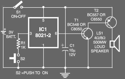
This simple circuit an low cost ding dong bell suitable for calling bell purposes. It is made around IC 8021-2 . IC 8021 has an in-built circuitry to produce ding dong sound each time its pin 3 is pulled low. The sound is stored in a 4 bit ROM.a complementary-pair, two-transistor amplifier is used to amplify the sound to a fair level of audibility. A piezo tweeter or an 8-ohm, 500mW speaker can be used at the output.

Ding dong bel Rumah

Skema Rangkaian bel Rumah

List Component bel Rumah:
R1: 1K 1/4W Resistance
C1: 10µF/12-25V Electrolytic Capacitance
T1: BC548/c8050 NPN transistor
T2: BC557/C8550 PNP transistor
IC1: 8021-2 ding dong sound generator
Ls1: Speaker tweeter 500 Mwatt - 5 watt
S1: switch on/off
S2: Switch Normally close
B1: 3V Cell

Each time when switch S2 is pressed, ding dong sound is produced twice. If you try to press switch S2 a second time when the first ding dong sound is still being produed, it has no effect whatever and the two ding-dong bell sounds will be invariably produced.S1 is the ON- OFF switch.Assemble the circuit on a good quality all pupose PCB.Don’t forget to use an IC holder for IC 8021.

IC 8021 Description

The 8021-2 is a ding-dong sound effect generator IC produced by LSI CMOS technology. With built-in RC oscillator and digital envelope circuits, minimal external components are required. This IC simulates the mechanical ding-dong sound, and is ideal for door bell application.

IC 8021 Features
- 1.3V to 3.3V operating voltage and low power consumption
- One-shot mode of 2 ding-dong playing sequences
- Standard TO-92 package form
- Dynamic speaker can be driven with external NPN transistor


IC 8021 Absolute Maximum Ratings
DC Supply Voltage ........................................... -0.3V to +5.0V
Operating Ambient Temperature .................... -10°C to 60°C
Storage Temperature ....................................... -55°C to 125°C


READMORE...

Rangkaian TDA 2616 Hi-fi Power Amplifier

This circuit is a 2X12 watt Hi-Fi Power amplifier circuit using IC TDA 2616 from Phillips. This circuit very Simple and robust circuit using very less components makes the circuit ideal for a portable power amplifier. The circuit delivers 12 W power on 8 Ohm speaker for each channel at +/- 12 V dual supply.
TDA 2616 Hi-fi Power Amplifier Skema Rangkaian TDA 2616 Hi-fi Power Amplifier

Note:
  • Capacitors except C10 & C9 are ceramic.
  • Capacitors Electrolic must be rated 50V.
  • Use a well regulated and filtered +/- 12 V dual power supply that is able to provide at least 2 A continuous current.
IC TDA2616 is a stereo power amplifier IC comes in a 9-lead single-in-line (SIL9) plastic power package (SOT131). This IC is specially designed for mains fed amplifier circuits, such as stereo radio,tape and television .The IC has good gain balance of both channels and Hi-fi in accordance with IEC 268 and DIN 45500 standards.


IC TDA 2616 DESCRIPTION

The TDA2616 is a hi-fi stereo amplifier designed for mains fed applications, such as stereo radio and TV. The circuit is optimally designed for symmetrical power supplies, but is also well-suited to asymmetrical power supply systems. An output power of 2 ´ 12 W (THD = 0.5%) can be
delivered into an 8 Wload with a symmetrical power supply of ±16 V. The gain is internally fixed at 30 dB, thus offering a low gain spread and a very good gain balance between the two amplifiers (0.2 dB). A special feature is the input mute circuit. This circuit disconnects the non-inverting inputs when the supply voltage drops below ±6 V, while the amplifier still retains its DC operating adjustment. The circuit features suppression of unwanted signals at the inputs, during switch-on and switch-off. The mute circuit can also be activated via pin 2. When a current of 300 mA is present at pin 2, the circuit is in the mute condition. The device is provided with two thermal protection circuits. One circuit measures the average temperature of the crystal and the other measures the momentary temperature of the power transistors. These control circuits attack at temperatures in excess of +150 °C, so a crystal operating temperature of max. +150 °C can be used without extra distortion.
IC TDA 2616 DESCRIPTION

READMORE...

Rangkaian Alarm LDR anti maling

Anti-theft alarm circuit it produces an audible alarm when fridge is left open for a preset time.Rangkaian This versatile alarm is based on two 555 timer IC's. Both ICS are wired as astable Multivibrators.An LDR is connected in parallel to the timing capacitor
C1 of IC 1.When is completely close door there will be no light inside the fridge and offers high resistance LDR R1 keeping fully charged.When door is left open, the lamp inside the fridge will remain glown, LDR will be illuminated, and its falls.This resistance makes
C1 stops charging and starts to discharge (In simple words, this is because at low resistance LDR bye passes much of the current in the parrallel path and capacitor gets less current). Now IC 1 starts oscillating slightly and after a preset time of 25 ( time T1) seconds high.This its output goes out put makes the Ic 2 to produce oscillations and results in a beeping sound for next 20 (time T2) seconds and cycle is repeated till door is closed.

 Alarm LDR  anti maling Skema Rangkaian Alarm anti maling


List Component alarm anti maling:
  • R1: 10K 1/4W Resistance
  • R3: 2.2 M 1/4W Resistance
  • R4: 1M 1/4W Resistance
  • C1: 10µF/25V Electrolytic Capacitance
  • C2: 100nF/63V Polyester Capacitance
  • D1: 1N4001 Diode
  • IC1,IC2: NE 555 Timer ICs
  • BZ1: Piezo Buzzer
  • B1: 3V Cell

Note:
Assemble the circuit on a good quality PCB .Time T1 & T2 can be adjusted by varying C1, C2, R1, R4 etc (Refer data sheet of 555). Place the LDR close enough to the lamp inside the fridge.

IC 555 Pin No Designation Description
 IC 555
  1. Ground, is the input pin of the source of the negative DC voltage
  2. Trigger, negative input from the lower comparators (comparator B) that maintain oscillation capacitor voltage in the lowest 1 / 3 Vcc and set RS flip-flop
  3. Output, the output pin of the IC 555.
  4. Reset, the pin that serves to reset the latch inside the IC to be influential to reset the IC work. This pin is connected to a PNP-type transistor gate, so the transistor will be active if given a logic low. Normally this pin is connected directly to Vcc to prevent reset
  5. Control voltage, this pin serves to regulate the stability of the reference voltage negative input (comparator A). This pin can be left hanging, but to ensure the stability of the reference comparator A, usually associated with a capacitor of about 10nF to berorde pin groun
  6. Threshold, this pin is connected to the positive input (comparator A) which will reset the RS flip-flop when the voltage on the capacitor from exceeding 2 / 3 Vc
  7. Discharge, this pin is connected to an open collector transistor Q1 is connected to ground emitternya. Switching transistor serves to clamp the corresponding node to ground on the timing of certain
  8. Vcc, pin it to receive a DC voltage supply. Usually will work optimally if given a 5-15V. the current supply can be seen in the datasheet, which is about 10-15mA.

READMORE...

Rangkaian Pembangkit Melody|Musik Mainan

Circuit of musik|melody generator you can make using an IC.The UM66 series are CMOS IC’s designed for using in calling bell, phone and toys. It has a built in ROM programmed for playing music. The device has very low power consumption.Thanks for the CMOS technology.The melody will be available at pin3 of UM66 and here it is amplified by using transistor Q1 dan Q2 to drive the speaker.

 Pembangkit Melody MainanSkema Rangkaian Pembangkit Melody Mainan

UM66 is a pleasing music generator IC which works on a supply voltage of 3V. the required 3V supply is given through a zener regulator. its out put is taken from the pin no1 and is given to a push pull amplifier to drive the low impedance lowd speker. A clss A amplifier before pushpull amplifier can be used to decrese the noise and improve out put. UM66 is a 3 pin IC pakage just looks like a BC 547 transistor.

Notes

  • Power supply must be between 6V - 15V .
  • Melody begins from the first note if power is reseted.
  • Assemble the circuit on a good quality common board.


IC UM66 Description
The U66 series is a CMOS LSI designed melody generator IC for use in telephones and toys application. It has an on-chip ROM programmed for musical performance. Produced by CMOS technology, the device results in very low power consumption. And with built-in RC oscillator, a compact melody module can be constructed with only a few additional components.

 IC UM66

Pin No Designation Description
-1. Out put Melody out put
-2. +Vdd Positive power supply
-3. -Vss Negative Power supply

Features of UM66T series
-62 Note ROM Memory
-Voltage rating: 1.3V to 3.3 V
-Power on reset
-

READMORE...

Saturday, August 22, 2009

Rangkaian Variable frequency oscillator

555 timer IC provides practical solutions and relatively inexpensive for a variety of electronic applications related to the timing (timing). Especially two of the most popular application is a series of monostable and astable timing. The main components of this IC consists of comparators and flip-flop is realized with a lot of transistors.

The principle component of this type of work does not change but each manufacturer makes the IC design and technology different. Almost all manufacturers make this type of component, although with a different. For example National Semiconductor LM555 call it, Philips and Texas Instruments SE/NE555 call. Motorola / ON-Semi designed with CMOS transistors that power consumption was small enough and called it MC1455. Philips and Maxim make his version of the CMOS ICM7555 name. Although different names, but the function of each diagram and pin compatible with each other. It's just that there are several different specific characteristics such as power consumption, maximum frequency and so on.

Variable frequency oscillator
Variable frequency oscillatorSkema Rangkaian Variable frequency oscillator

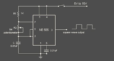
HereNE55 is wired as an astable multivibrator ,whose out put frequency can be varied by varying a potentiometer.This circuit is a must in the work bench of a electronic hobbyist.Frequencies ranging from several Hz to several KHz can be obtained using this circuit.For very low frequencies (few Hz) replace C with a higher value electrolytic capacitor.

The values of R and C can be obtained using the following equations.

1/f = 0.69 * C * ( R1 + 2*R2).

% duty cycle = 100*(R1+R2)/(R1+ 2*R2) .

The good option is to select R1 in K Ohms and R2 in M Ohms.


READMORE...

Friday, August 21, 2009

Rangkaian Ic 4060 Timer Dengan Alarm

The IC 4060 is a 14-stage ripple-carry binary counter/divider and oscillator with three oscillator terminals (RS, RTC and CTC), ten buffered outputs (O3 to O9 and O11 to O13) and an overriding asynchronous master reset input (MR). The oscillator configuration allows design of either RC or crystal oscillator circuits. The oscillator may be replaced by an external clock signal at input RS. The counter advances on the negative-going transition of RS.
A HIGH level on MR resets the counter (O3 to O9 and O11 to O13 = LOW), independent of other input conditions. Schmitt-trigger action in the clock input makes the circuit highly tolerant to slower clock rise and fall times.

Rangkaian Timer Dengan AlarmRangkaianIc 4060 Timer Dengan Alarm

A timer circuit using IC 4060 is given here. The IC 4060 is a 14 stage binary counter with a built-in oscillator.R2, R7, C1 are the components that determine the frequency of the oscillator and the outputs will become high one after other and only one at a time. The last five outputs are only used here. The high pulses from the outputs are used to trigger the NE555 IC. Here NE555 is wired as a monostable multivibrator. The buzzer will produce the alarm when the output of IC2 goes high. The duration of the alarm depends on the components C3 and R5.The duration can be adjusted by varying the value of C3.The alarm will automatically turn OFF after the predetermined time. The trigger pin of IC2 will be normally positive. When the Q1 is forward biased by the positive pulse at its base from IC1, the capacitor C2 becomes charged and reduces the voltage at trigger pin of IC2.This triggers the IC.When the capacitor is fully charged the pin 2 becomes again positive.
The maximum duration from timer IC 4060 will be at pin 3. The times decrease by half in the pins 2, 3, 15, and 13 respectively. The timer duration can be varied by varying the capacitor C1.

Notes
  • Use 6V DC for powering the circuit.
  • Mount the ICs on holders.
  • The switch S2 can be a single pole five throw rotary switch.
  • The switch S1 can be a push button switch.
  • S1 is used to reset the timer.
  • S2 is used to select the alarm time.
  • R7 can be used for the fine adjustment of alarm time.

READMORE...

Thursday, August 20, 2009

Skema 2N3055 Power Amplifier

Amplifier power is a series of electronics that is used to strengthen the power (or energy in general). In the field of audio, amplifier will amplify the sound signal (which has been expressed in the form of electric current) on the input it into electric current is stronger at the output. The amount of strengthening is often known by the term gain. Value of the gain is expressed as a function of frequency is called the transfer function.

So the gain is the result of the power output (Pout) and power at the input to its function in the form of frequency. The size of the gain, (G) is usually the Decibel (dB).

2N3055 Power Amplifier

Skema 2N3055 Power Amplifier. The optimal supply voltage is around 30V, but this amp work from 24 to 32V. The maximal input voltage is around 0.8 - 1V. As you can see, in this design the components have a big tolerance, so you can build it almost of the components, which you find at home. The and transistors can be any NPN type power transistor, but do not use Darlington types. The output power is around 150 Watt.

Amplifier schematic:
2N3055 Power AmplifierSkema Rangkaian 2N3055 Power Amplifier

capacitor C1 regulates the low frequencies (bass), as the capacitance grows, the low frequncies are getting louder.

capacitor C2 regulates the higher frequencies (treble), as the capacitance grows, the higher frequencies are getting quiter.

this is a class B amplifier, this means, that a current must flow through the end transistors, even if there is no signal on the input. This current can be regulated with the 500Ω trimmer resistor. As this current incrases, the sound of the amplifier gets better, but the end transistors are more heating. But if this current decrases, the transistors are not heating so much, but the sound gets worse.

READMORE...

Skema LM3886 68 Watt Audio Power Amplifier

Skema Rangkaian LM3886 68 Watt Audio Power Amplifier


The LM3886 is a high-performance audio power amplifier capable of delivering 68W of continuous average power to a 4 load and 38W into 8 with 0.1% THD+N from 20Hz-20kHz.

The performance of the LM3886, utilizing its Self Peak Instantaneous Temperature (°Ke) (SPiKe™) protection circuitry, puts it in a class above discrete and hybrid amplifiers by providing an inherently, dynamically protected Safe Operating Area (SOA). SPiKe protection means that these parts are completely safeguarded at the output against overvoltage, undervoltage, overloads, including shorts to the supplies, thermal runaway, and instantaneous temperature peaks.

The LM3886 maintains an excellent signal-to-noise ratio of greater than 92dB with a typical low noise floor of 2.0µV. It exhibits extremely low THD+N values of 0.03% at the rated output into the rated load over the audio spectrum, and provides excellent linearity with an IMD (SMPTE) typical rating of 0.004%.
 LM3886  68 Watt  Audio Power Amplifier
Gambar Skema LM3886 68 Watt Audio Power Amplifier

Notice:
  • 68W cont. avg. output power into 4 at VCC = ±28V
  • 38W cont. avg. output power into 8 at VCC = ±28V
  • 50W cont. avg. output power into 8 at VCC = ±35V
  • 135W instantaneous peak output power capability
  • Signal-to-Noise Ratio >= 92dB
  • An input mute function
  • Output protection from a short to ground or to the supplies via internal current limiting circuitry
  • Output over-voltage protection against transients from inductive loads
  • Supply under-voltage protection, not allowing internal biasing to occur when |VEE| + |VCC| <= 12V, thus eliminating turn-on and turn-off transients
  • 11-lead TO-220 package
  • Wide supply range 20V - 94V
 LM3886  68 Watt  Audio Power Amplifier

READMORE...

Monday, August 17, 2009

Rangkaian Pemancar TV Sederhana

This Rangkaian Pemancar TV uses standard 1 FM modulation for sound and PAL for video modulation. Audio signal will be modulated is pre-amplified using the transistor Q1 and associated components. The transistor Q2 has two jobs: production of carrier frequency and modulation. The pre-amplified audio signal is fed to the base of transistor Q2 for modulation. Capacitor C5 and inductor L1 forms the tank circuit which is responsible for producing the carrier frequency. The video signal is fed to the emitter of transistor Q2 via POT R7 for modulation. The modulated composite signal (audio+video) is transmitted by the antenna A1.

 Pemancar TV  Skema Rangkaian Pemancar TV Sederhana

Inductor L1 can be made by making 4 turns of 24SWG enameled copper wire on a 6mm dia: plastic former. T1 can be a radio frequency transformer with built in capacitor. (Can be found on old transistor radio boards). Antenna A1 can be a 1M long copper wire. (Experiment with the length to get optimum performance). This transmitter is working in VHF band somewhat between 50 – 210MHz. This transmitter is compatible only with PAL B and PAL G systems.

List Componet:
R1 = 10KOhm R2 = 47KOhm R3 = 15KOhm R4 = 8.2KOhm R5 = 47KOhmR6 = 47KOhm R7 = 1Kohm resistor variable R8 = 75Ohm C1 = 10uF/25Volt capacitor electrolik C2 = 0.001uf/10nF capacitor ceramic C3 = 100nF C4 = 10nf C5 = 47pF (variable capacitor) C6 = 10nF C7 = 10pF C8 = 27pF c9 = 100nF C10 = 470uF c11 = 10nF C12 = 220uF/25Volt Q1 = BC547 NPN transistor Q2 = BC547 NPN transistor
T1 = T1 can be a radio frequency transformer with built in capacitor. (Can be found on old transistor radio boards).
L1 = 4 turns of 24SWG enameled copper wire on a 6mm dia: plastic former.

READMORE...

Rangkaian +5V Switching regulator

Rangkaian +5V Switching regulator used LM2575-5.0. You can make the stable voltage by using the 3 terminal regulator like LM317. However, because the output electric current and the inputted electric current are the same approximately, the difference between the input electric power (The input voltage x The input electric current) and the output power (The output voltage x The output current) is consumed as the heat with the regulator. Because it is, the efficiency isn’t good. In case of the switching regulator, it inputs only the electric power which is necessary to output from the input by the switching operation. Because it is, there is little electric power to consume with the regulator and it is efficient.


Switching regulator
Skema Rangkaian +5V Switching regulator

DC to DC step down voltage regulator. Wide input voltage 8Vdc to 40Vdc.
  • LM2575-3.3 (3.3Vdc output)
  • LM2575-5.0 (5Vdc output)
  • LM2575-12 (12Vdc output)
  • LM2575-15 (15Vdc output)
  • LM2575-ADJ (1.23Vdc to 37Vdc output)

The switching regulator which introduces in this page is the step down type and is the one to get the output voltage which is lower than the input voltage. As for the regulator which uses this time, the output is 5-V fixation.
The switching regulator of the step up type can be made the voltage which is higher than the input voltage.


Kegunaan IC LM2575

The LM2575 series of regulators are monolithic integrated circuits that provide all the active functions for a step-down (buck) switching regulator, capable of driving a 1A load with excellent line and load regulation. These devices are available in fixed output voltages of 3.3V, 5V, 12V, 15V, and an adjustable output version.

Requiring a minimum number of external components, these regulators are simple to use and include internal frequency compensation and a fixed-frequency oscillator.

The LM2575 series offers a high-efficiency replacement for popular three-terminal linear regulators. It substantially reduces the size of the heat sink, and in many cases no heat sink is required.

A standard series of inductors optimized for use with the LM2575 are available from several different manufacturers. This feature greatly simplifies the design of switch-mode power supplies.

Other features include a guaranteed ±4% tolerance on output voltage within specified input voltages and output load conditions, and ±10% on the oscillator frequency. External shutdown is included, featuring 50 μA (typical) standby current. The output switch includes cycle-by-cycle current limiting, as well as thermal shutdown for full protection under fault conditions.

READMORE...

Rangkaian Audio Mixer 3 Input

Many audio mixer circuits have been published but this this very simple audio mixer circuit uses only one transistor. The base emitter junction of the transistor is biased by the diodes D1 and D2.The signals to be mixed are directly coupled to the base of Transistor. Each input lines are current limited by using a 10k Potensiometer . With the used component values the collector current is around 1mA.
Audio MixerSkema Rangkaian Audio Mixer 3 Input

Notice:
  • The circuit can be assembled on a Vero board.
  • The circuit can be powered from 9-25V DC.
  • of each channel can be set using Variable resistor 10k

Transistors in the following series is enabled as a source of constant flow. By providing input audio signal on the emitter, the voltage on the emitter will fluctuate, which will cause the collector voltage also fluctuates. The amount of frequency fluctuation is comparable with the frequency of the incoming audio signal.

READMORE...

Rangkaian Remote Control IC 555

Remote Control menggunakan IC 555

Ic 555 is an integrated circuit (chip) implementing a variety of timer and multivibrator applications. The IC was designed by Hans R. Camenzind in 1970 and brought to market in 1971 by Signetics (later acquired by Philips). The original name was the SE555 (metal can)/NE555 (plastic DIP) and the part was described as "The IC Time Machine". It has been claimed that the 555 gets its name from the three 5-kohm resistors used in typical early implementations, but Hanz Camenzind has stated that the number was arbitrary The part is still in wide use, thanks to its ease of use, low price and good stability. As of 2003 it is estimated that 1 billion units are manufactured every year.

Depending on the manufacturer, the standard 555 package includes over 20 transistors, 2 diodes and 15 resistors on a silicon chip installed in an 8-pin mini dual-in-line package (DIP-8).

The 556 is a 14-pin DIP that combines two 555s on a single chip. The 558 is a 16-pin DIP that combines four slightly modified 555s on a single chip (DIS & THR are connected internally, TR is falling edge sensitive instead of level sensitive).

Also available are ultra-low power versions of the 555 such as the 7555 and TLC555. The 7555 requires slightly different wiring using fewer external components and less power.


The connection of ic 555 as follows:
  • GND(1)Ground, low level (0V)
  • TRIG(2)A short pulse high-to-low on the trigger starts the timer
  • OUT(3)During a timing interval, the output stays at +VCC
  • RESET(4)A timing interval can be interrupted by applying a reset pulse to low (0V)
  • CTRL (5)Control voltage allows access to the internal voltage divider (2/3 VCC)
  • THR (6)The threshold at which the interval ends (it ends if U.thr → 2/3 VCC)
  • DIS (7)Connected to a capacitor whose discharge time will influence the timing interval
  • V+, VCC(8) The positive supply voltage which must be between 3 and 15 V

READMORE...

Saturday, August 15, 2009

Rangkaian Radio Remote Control Mobil Mainan

Rangkaian Remote Control Mobil Mainan

In this system, radio signals emanated not continue to be raised but only when the controller sends the right / left or forward / backward, that is only a radio frequency that discontinuous,so that the credit delivery frequency radio waves.

The amount of credit that is sent to represent the command post, the forward was represented with 8 credits, left represented with 16 credits, 32 credits right and Backward 64 credits. Commands can be sent is a combination of 2 commands, namely the combination of forward / backward and right / left, as an example can be sent forward and the left, in this case the amount of credit that is sent 24, the Answer of the forward and the balance of 8 the left as many as 16 credits.


Making transformer TX and RX:
Transformer T1 in series transmitter and recipient, is the same, and must be made. Transformer was built using plastic koker transformer (spare part radio) so that the step appears to have 5 channels that can be filled with a wire coil, as shown in the picture. Wearing this koker facilitate scrolling wire transformer. If it can not be koker like that, just use the normal. Koker transformer is small and ferit is also small (3 mm) as the first assembly is often used for CB 27 MHz radio.

Transformer wire to wire to use in the unloading of koker, and slowly open the wire coil inside the existing wire koker because it is quite smooth and easy to drop out
  • coil wire from the foot of the number to 5 feet 4 hours direction (CW) of 3-and-roll at level 1 (line at the bottom line above)
  • Scroll through the wire from 1 foot to 2 feet clockwise roll of 4 on the exact level 2.
  • Continue to roll (from step 2) clockwise a quarter roll of 3 to 3 feet in three levels. (You can set exactly a quarter roll, because the path that has kokernya be split into 4).
Making coil L1
Scroll through the copper wire diameter size of 0.3 - 0.5 mm of 10 quarter roll koker in diameter about 4 mm (which will be released later) is also clockwis

Making coil L2
Scroll through the copper wire diameter of 0.1 mm sizes of 50 on the roll without koker plastic ferit diameter about 3.5 - 4 mm (search item from the plastic material used) is also clockwise. The length of the coil along liputi in 5 mm.

READMORE...

Control Lampu|kipas Angin 200 watt/220 volt

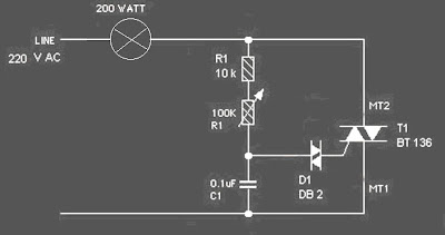
Rangkaian Control Lampu|kipas Angin is the circuit diagram of the simplest lamp dimmer or fan regulator.The circuit is based on the principle of power control using a Triac.The circuit works by varying the firing angle of the Triac . Resistors R1 ,R2 and capacitor C2 are associated with this.The firing angle can be varied by varying the value of any of these components.Here R1 is selected as the variable element .By varying the value of R1 the firing angle of Triac changes (in simple words, how much time should Triac conduct) changes.This directly varies the load power, since load is driven by Triac.The firing pulses are given to the gate of Triac T1 using Diac D1.

circuit of lamp dimmer regulatorSkema Rangkaian Control Lampu|kipas Angin


Component List:
  • R1 : 1o K (1 Watt Resistor)
  • R2 : 1o0 K ( Potentiometer)
  • C1 : 0.1 uF /500V (Polyester Capacitor)
  • T1 : BT 136 (Triac)
  • D1 : DB2 (Diac)
Assemble the circuit on a good quality PCB or common board.The load whether lamp ,fan or any thing ,should be less than 200 Watts.To connect higher loads replace the Triac BT 136 with a higher Watt capacity Triac . All parts of the circuit are active with potential shock hazard.So be careful.

to avoid the occurrence that is not in want, when you try to light a flame controller circuit, the voltage should use a small first, such as 12 volt and small lamps 12 volt of circulating in many shops electronic. when circuit can work well, a circuit of Control Lampu|kipas Angin can use the voltage 220 volt with max load 200 watts.

READMORE...

Rangkaian Pengusir Nyamuk

This is a circuit diagram of an ultrasonic mosquito repeller (pengusi yamuk). The circuit is based on the theory that insects like mosquito can be repelled by using sound frequencies in the ultrasonic (above 20KHz) range. The circuit is nothing but a PLL IC CMOS 4047 wired as an oscillator working at 22KHz. A complementary symmetry amplifier consisting of four transistor is used to amplify the sound. Speaker Piezo buzzer converts the output of amplifier to ultrasonic sound that can be heard by the insects.
Rangkaian Pengusir Nyamuk
Skema Rangkaian Pengusir Nyamuk

The circuit can be powered from 12V DC. The buzzer can be any general purpose piezo buzzer.

Description IC CD4047B

IC CD4047B is capable of operating in either the monostable or astable mode. It requires an external capacitor (between pins 1 and 3) and an external resistor (between pins 2 and 3) to determine the output pulse width in the monostable mode, and the output frequency in the astable mode. Astable operation is enabled by a high level on the astable input or low level on the astable input. The output frequency (at 50% duty cycle) at Q and Q outputs is determined by the timing components. A frequency twice that of Q is available at the Oscillator Output; a 50% duty cycle is not guaranteed. Monostable operation is obtained when the device is triggered by low-to-high transition at a trigger input or high-tolow transition at b trigger input. The device can be retriggered by applying a simultaneous low-to-high transition to
both the a trigger and retrigger inputs. A high level on Reset input resets the outputs Q to low, Q to high.
Lay out IC CD4047B

Block and Connection Diagrams IC CD4047B

IC CD4047B Applications

Frequency discriminators
Timing circuits
Time-delay applications
Envelope detection
Frequency multiplication
Frequency division

READMORE...

Friday, August 14, 2009

Rangkaian Pendeteksi (Sensor) Kelembaban Udara

Pendeteksi (Sensor) Kelembaban Udara

Dew ad- versely affects the normal per- formance of sensitive electronic devices. A low-cost circuit described here can be used to switch off any gadget automatically in case of excessive humidity. At the heart of the circuit is an inexpensive (resistor type) dew sensor element. Although dew sensor elements are widely used in video cassette players and recorders, these may not be easily available in local market. However, the same can be procured from authorised service centres of reputed companies. The author used the dew sensor for FUNAI VCP model No. V.I.P. 3000A (Part No: 6808-08-04, reference no. 336) in his prototype. In practice, it is observed that all dew sensors available for video application possess the same electrical characteristics irrespective of their physical shape/size, and hence are interchangeable and can be used in this project.


Pendeteksi (Sensor) Kelembaban Udara
Skema Rangkaian Pendeteksi (Sensor) Kelembaban Udara


The circuit is basically a switching type circuit made with the help of a popular dual op-amp IC LM358N which is configured here as a comparator. (Note that only one half of the IC is used here.) Under normal conditions, resistance of the dew sensor is low (1 kilo-ohm or so) and thus the voltage at its non-inverting terminal (pin 3) is low compared to that at its inverting input (pin 2) terminal. The corresponding output of the comparator (at pin 1) is accordingly low and thus nothing happens in the circuit. When humidity exceeds 80 per cent, the sensor resistance increases rapidly. As a result, the non-inverting pin becomes more positive than the inverting pin. This pushes up the output of IC1 to a high level. As a consequence, the LED inside the opto-coupler is energised. At the same time LED1 provides a visual indication. The opto-coupler can be suitably interfaced to any electronic device for switching purpose. Circuit comprising diode D2, resistors R5 and R6 and capacitor C1 forms a low-voltage, low-current power supply unit. This simple arrangement obviates the requirement for a bulky and expensive step-down transformer.

READMORE...

Rangkaian Alarm pendeteksi Api menggunakan LDR

In the rooms are vulnerable to fire, such as a storage material flammable, required a system of prevention of the occurrence of fire. For example, using a fire alarm, so that eg arise if a flame, can be quickly and by others that can immediately fire it does not cause a fire is greater.

Here is a simple fire alarm circuit based on a LDR and lamp pair for sensing the fire.The alarm works by sensing the smoke produced during fire.The circuit produces an audible alarm when the fire breaks out with smoke.

Fire alarm circuit Skema rangkaian alarm pendeteksi api|kebakaran

Note:
  • The speaker can be a 8Ω tweeter.
  • POT R4 can be used to adjust the sensitivity of the alarm.
  • POT R3 can be used for varying the volume of the alarm.
  • Any general purpose NPN transistor( BC548,BC148,2N222) can be used for Q1.
  • The circuit can be powered from a 9V battery or a 9V DC power supply.
  • Instead of bulb you can use a bright LED with a 1K resistor series to it.

When there is no smoke the light from the bulb will be directly falling on the LDR.The LDR resistance will be low and so the voltage across it (below .6V).The transistor will be OFF and nothing happens.When there is sufficient smoke to mask the light from falling on LDR, the LDR resistance increases and so do the voltage across it.Now the transistor will switch to ON.This gives power to the IC1 and it outputs 5V.This powers the tone generator IC UM66 (IC2) to play a music.This music will be amplified by IC3 (TDA 2002) to drive the speaker.

The diode D1 and D2 in combination drops 1.4 V to give the rated voltage (3.5V ) to UM66 .UM 66 cannot withstand more than 4V.

READMORE...

Rangkaian Sekring|Fuse Otomatis

To restrict / security, electric current is usually used fuse/sekring or patron is dissolved when going short (konslet) will drop out and must be replaced with a new one. Then, in order not to drop out of each new change means that more money out to buy, then there fuse/sekring automatically work with the reset button. So there are problems with each short, fuse/sekring will automatic decided flow then to return it does not need to buy a new (if not broken) just press the reset the equipment will live again.

This is one of the simplest electronic fuse circuit one can make. The circuit uses only one transistor, one SCR, one push button switch and two resistors.

Simple electronic fuse
Skema Rangkaian Sekring|Fuse Otomatis


The value of R1 can be obtained from the equation; [Imax] X [R1] = 0.7V.
R2 can be obtained from the equation; R2 = [Vs] X [1K Ohms].
Wattage rating of R1 can be obtained from the equation; W = [Imax] X [Imax] X [R1].
For this circuit to work the current consumption of the load must be greater than the holding current of the SCR.

The working of the circuit is very simple. Initially the load current flows through SCR and resistor R1.The value of R1 is so selected that, the maximum load current multiplied by the resistance of R1 is equal to 0.7 volts. When the load current exceeds the maximum value the voltage drop across R1 becomes more than 0.7V and switches transistor Q1 ON. Now the transistor completely bye passes the load current and the current through triac falls below the holding current. This makes the triac OFF. When SCR is OFF there will not be any current flow through R1 and so the voltage across it falls to 0.This makes the transistor OFF, completely isolating the load circuit.The fuse can be resetted by pressing S1.When S1 is pressed the SCR is again triggered and remains latched to conduct the load current.


READMORE...

Rangkaian Regulator menggunakan Op-Amp

Regulator is a series of regulations or the voltage output from power so that a portion darinaik effects or voltage drop in net does not affect the voltage ration power to be so stable.


Regular circuit of regulators have been good if the ripple voltage is small, but there is a problem of stability. If the voltage PLN rise /down, then the output voltage is also will be rise /donw. regular circuit of regulators, if the current of the larger, the dc voltage output is also down. For some applications this voltage change will very disrupt.

Rangkaian Regulator menggunakan Op-Amp


Regulator using Op-AmpSkema rangkaian regulator menggunakan OP-Amp

Technical regulations that better is to use the Op-Amp for a drive-transistor Q. Dioda zener here do not give directly to the bait transistor Q, but as a reference voltage for the Op-Amp IC1. Feedback on the negative pin Op-amp is a snippet from the voltage regulator out, namely:
Regulator using Op-AmpIf the voltage V out exit Ascending, voltage V in (-) also Ascending until this voltage is the same as the reference voltage Vz. Likewise if the voltage V out decreases exit, for example because of supply current to the load increases, Op-amp will maintain stability in the V reference point z with the current IB to the transistor Q1 so that at any time in the Op-amp maintain stability:
Regulator using Op-Amp
Ignore the VBE voltage transistor Q1 and mensubsitusi formula, obtained by mathematical relationships
Regulator using Op-Amp
In the circuit of regulator Op-Amp of this output voltage can be adjusted with the set of R1 and R2.

READMORE...

Wednesday, August 12, 2009

Rangkaian Regulator menggunakan Diode Zener

Regulator is a circuit of regulations or the voltage output from a ration resources so that the effects of increased tension or decrease in net does not affect the voltage ration power to be so stable.


Rangkaian Dasar Regulator Diode Zener

Simple circuit regulator , working on the zener breakdown voltage so that it produces the same output with the zener voltage, however, this circuit is only useful if the current burden of not more than 50mA. simple circuit regulator using zener diode can you see in the circuit under the scheme

Circuit of regulator using diode Zener
Skema rangkaian Regulator Dioda Zener dasar

voltage output:
Rangkaian regulator Diode ZenerResistor value
Circuit of regulator using diode ZenerWith this design approach, you must check the power ratings of your output resistor and Zener diode to make sure they are able to handle the power requirements.

The power rating load of resistor and zener diode must be at least of they are able to handle
Rangkaian Regulator Zener dengan Transistor

Regulator This is basically the zener regulator is configured with an NPN transistor to produce a large amount of cash. V BE is the base-voltage emitor of the size of the transistor Q1 between 0.2 - 0.7 volt depending on the type of transistor used. By ignoring the current IB flowing in the transistor base, can be counted prisoners of R2 that is needed is:

Circuit of regulator using diode Zener
Rangkaian regulator Diode Zener
Skema rangkaian Regulator menggunakan Diode Zener

Iz is a minimum flow required by dioda to reach the zener voltage is zener breakdown. Large currents can be known from the datasheet that the size of the approximately 20 mA

If the required portion of greater flow, calculation of base flow in the IB on the circuit can not be ignored anymore. As is known, large currents IC akan proportionate flow straight to the IB or with the right formula

Rangkaian regulator Diode ZenerFor such purpose, the transistor Q1 can be replaced with a Darlington tansistor usually have a value of b is quite large. With the Darlington transistor, the base flow of small currents can produce a larger IC

READMORE...
 
Skema Rangkaian Elektronika