Saturday, October 24, 2009

Rangkaian Power Amplifier BTL

Power Amplifier BTL

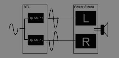
Audio amplifiers operate either in a BTL (bridged) or single-ended ("normal") configuration. In the single-ended setup, the output lead goes to the "hot" or "+" side of the load (speaker or speaker box since we are talking audio) and the "-" or "negative" side of the load is tied to a common ground shared with the amplifier. In the BTL configuration, one amp is connected to the "+" side of the speaker (load) and a second amp is connected to the "-" side of the load. For this to work, the output signal from the second amplifier must be a "mirror image" (identical in every respect, but 180 degrees out of phase) of the output from the first amp. The BTL configuration is most often seen in low-voltage, battery-powered applications (like cell phones or "walkman" type personal tape or cd players etc) or in automotive applications over about 10 watts per channel.

In the BTL configuration, each amp drives half the load impedance. With the signals being out of phase, the voltage swing across the load appears to be doubled, and with each amp driving half the impedance the current is doubled. In theory the bridged pair will produce 4 times the power into the load that either amp acting alone could provide. In reality it seldom works that well.

This is an power amplifier circuit of a BTL system, which comprises a first op-amp chip which outputs an output signal having a same phase as an input signal input to a signal input terminal, a second operational amplifier which outputs an output signal having an opposite phase to the input signal, a voltage divider which generates a midpoint voltage of the input signal, a first resistor connected between an output terminal and a negative phase input terminal of the first operational amplifier, second and third resistors connected in series between the negative phase input terminals of the first and second operational amplifiers, a fourth resistor connected between an output terminal and the negative phase input terminal of the second operational amplifier, and an impedance converter connected between a midpoint voltage node of the voltage divider and a series-connection node of the second and third resistors. (end of abstract)


Power Amplifier BTL


List Componet:
R1, R2,R3, R4, R6..................... 10kOhm.
R3............................................. 20kOhm.
C1, C2, C3, C4........................... 10µF.
Catu daya (VCC) ±12 V.
.

READMORE...

Friday, October 16, 2009

Rangkaian Pre-Amp Mic 2 Transistor.

Here is a Pre-amp microphone dynamic using two transistors. The circuit factor of this around 150 and can handle signals from 50Hz to 100Khz.This circuit is designed for use with 200 Ohm dynamic microphones. For usage with low impedance microphones, the value of R3 must be increased to around 47o Ohms and C1 must be decreased to around 2.2uF.

Pre-Amp mic 2 transistorSkema rangkaian Pre-Amp mic 2 transistor

The audio signal from the microphone is coupled to the base of Q1 via the capacitor C1 and resistor R3. Q1 works as a preamplifier here. The preamplified signal will be coupled to the base of Q2 for further amplification. Resistor network comprising of R4, R5 and R6 provides the necessary negative feedback. Final output signal will be available at the emitter of Q2.


Layout Transistor BC549 & BC546

Transistor BC549 Absolute maximum rating
  • VCBO collector-base voltage open emitter...............30 V.
  • VCEO collector-emitter voltage open base...............30 V.
  • VEBO emitter-base voltage open collector................5 V.
  • IC collector current (DC)........................................100 mA.
  • ICM peak collector current......................................200 mA.
  • IBM peak base current............................................200 mA.
  • Ptot total power dissipation Tamb £ 25 °C..................500 mW.
  • Tstg storage temperature...................................... -65 to +150 °C.
  • Tj junction temperature..........................................150 °C.
  • Tamb ambient temperature..................................... -65 to +150 °C.
  • hFE DC current gain VCE = 5 V, IC = 2 mA .............420 to 800.

Transistor BC546 Absolute maximum rating
  • VCBO collector-base voltage open emitter..................80 V.
  • VCEO collector-emitter voltage open base..................65 V.
  • VEBO emitter-base voltage open collector..................6 V.
  • IC collector current (DC).........................................100 mA.
  • ICM peak collector current.......................................200 mA.
  • IBM peak base current.............................................200 mA.
  • Ptot total power dissipation Tamb £ 25 °C.................. 500 mW.
  • Tstg storage temperature........................................ -65 +150 °C.
  • Tj junction temperature...........................................150 °C.
  • Tamb operating ambient temperature ........................-65 +150 °C.
  • hFE DC current gain VCE = 5 V, IC = 10 mA..............150.

READMORE...

Rangkaian Treble boost

This is Treble Boost circuit. IC LM741 that excellent like to use general the price economizes , and use electronics other equipment assemble a little. In this circuit has can to improve the treble about 10000 Hz that 40 dB. By you can change C1 be other value as a result , will affect the treble differently. This circuit uses the fire feeds about 9V. See the circuit and read to add.


treble boostSkema rangkaian treble boost


Note:
  • Use 12V to 16 VDC for powering the circuit.
  • Mount IC1 on a holder.
  • C3,C3,c4 and C5 must be rated at least 25V.

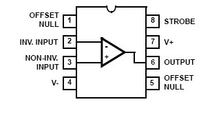
IC Op-Amp LM741

The LM A741 is a high performance monolithic operational amplifier constructed on a single silicon chip. It is intented for a wide range of analog applications.


Absolute maximum rating

Supply voltage (VCC) ±22 V.
Differential Input Voltage (Vid ) ±30 V.
Input Voltage (Vi ) ±15 V.
Power Dissipation (Ptot) 500 mW.
Storage Temperature Range (Tstg) -65 to +150 °C.
.

READMORE...

Rangkaian Sound Effects Generator

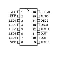
This is a sound effects generator circuit used IC HT2884. There are 8 different sound effect can be produced that are 2 lazer guns, 1 dual tone horn sound, 2 bomb sounds, 2 machine gun sounds and a rifle shot sound.


Sound Effects Generator Skema rangkaian sound effects generator

Power is a 3 Volt battery, but the IC will work with any voltage between 2.5 - 5 Volts. Switch S1 is the on / off switch. The output at pin 10 is amplified and drives a small 8 ohm loudspeaker. Pressing S3 once will generate all the sounds, one after another. S2 can be used to produce a single sound effect, next depression gives the next sound effect. Standby current is about 1 uA at 3 Volt, so battery life is very economical.


IC HT2844 Description

The IC HT2844 is a CMOS LSI chip designed for use in sound effect products. It is equipped with tone circuit, noise circuit, and other control logic to generate various sounds including rifle gun, machine gan, booming, door bell, alarm, and so forth. the feature of the customer's sound source can be analyzed and programmed into an internal ROM by changing a mask layer durimg device fabrication

IC HT2844
Absolute maximum rating
Supply voltage....................................... 03 to 5 Volt.
Input voltage.......................................... Vss - 0.3 to VDD+0.3 Volt.
Storage temperature.............................. -50 to 125 C.
Operating temperature........................... 0 to 70 C.
.

READMORE...

Wednesday, October 14, 2009

Rangkaian Car Regulator Converter

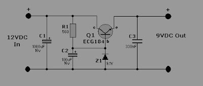
This is car regulator 12 VDC to 9 VDC converters side for audio, playstation,DVD,etc... The regulator designed for 12DC to 9DC converters that we bring to our design circuit . They are all effective in Switch Mode Power Supplies regulated output. We have developed a series of DC-DC power supply models ranging from 1 watt to 500 watts, which we incorporated into the new controller of DC converters. We are also developing new areas whenever necessary to meet customer requirements. We can provide some custom products that changes on the following products and fully custom DC-DC, new products, such as DC Battery Backup Power Supplies.


car regulator converter
Note:
Assemble the circuit on a good quality PCB.
The Q1 ECG184 must be mounted on heat sinks.


list Componet

C1: 1000uf/16v
C2: 100uf/16v
C3: 330nf
R1: 560 ohm, Resistor 1 watt
Z1: 9.1 Volt, diode zener
Q1: EGC184.
.

READMORE...

Rangkaian Sirine Sederhana 2 Transistor

This is a simple Siren circuit used 2 transistor . The siren circuit produced imitates the rise and fall of an American police siren. When first switched on the 10u capacitors is discharged and both transistors are off. When the push button switch is pressed to 10u capacitor will charge via 22k resistor. This voltage is applied to the base of the BC108B which will turn on slowly. When the switch is released the capacitor will discharge via the 100k and 47k base resistors and the transistor will slowly turn off. The change in voltage alters the frequency of the siren.

Sirine Sederhana
Skema rangkaian sirine sederhana

Current drain is fairly high in this circuit so a suitable power supply is required. The duration the tone takes to rise and fall is determined by the 10u and 22k resistor. These values may be varied for different effects.


Transistor 2N3702 description

This device designed for use as PNP general purpose amplifier and switches requiring collector currents to 300mA.


Absolute Maximum Ratings
  • Collector-Emitter Voltage (VCEO ): -25 V.
  • Collector-Base Voltage (VCBO ): -40 V.
  • Emitter-Base Voltage (VEBO ): -5.0 V.
  • Collector Current - Continuous (IC): -500 mA.
  • Operating and Storage Junction Temperature Range (TJ, TST): -55 ~ +150 C.
  • Current Gain (hFE DC ): 60 - 300.


Pin transistor BC 108
  • Low current (max. 100 mA).
  • Low voltage (max. 45 V).
  • Current Gain (hFE DC) : 110 - 450.

.

READMORE...

Monday, October 12, 2009

Rangkaian Mini FM Radio Transmitter

This is an mini fm Radio transmitter circuit. The supply voltage is between 1.1 – 3 Volts with power consumption is 1.8 mA at 1.5 Volts. This circuit should be able to cover 30 meters of range max. at 1.5 Volts.

mini FM transmitterSkema rangkaian mini FM transmitter


Note:
* Use a battery for powering the circuit.It will reduce noise.
* An FM antenna from a old radio is a better option than the wire antenna.


PN2222A transistor description

This device is NPN General Purpose Amplifier for use as a medium power amplifier and switch requiring collector currents up to 500mA.

Absolute Maximum Ratings.
  • Collector-Emitter Voltage (VCEO ) : 40 V.
  • Collector-Base Voltage (VCBO) : 75 V.
  • Emitter-Base Voltage (VEBO) : 6.0 V.
  • Collector Current (IC) 1.0 : A.
  • Operating and Storage Junction Temperature Range (TSTG) :- 55 ~ 150 °C.
  • Collector-Emitter Breakdown Voltage : 40 V.
  • Collector-Base Breakdown Voltage : 75 V.
  • Emitter-Base Breakdown Voltage : 6.0 V.

READMORE...

Sunday, October 11, 2009

Rangkaian Pembangkit Suara Burung

This generate a sound like bird’s circuit. The trafo LT700 is a small audio transformer with primary is center tapped with an impedance of 1Kohms at 1KHz . The secondary has an impedance of 8 ohms.

 Pembangkit Suara BurungSkema rangkaian pembangkit suara burung


The inclusion of R1 and C1 give this oscillator its characteristic “chirp”. As the 100u capacitor charges via the 4.7K resistor, R1 the bias for the transistor is cut off. This causes the oscillation to stop, the capacitor discharges through the base emitter circuit of the transistor and oscillations start again. Altering these components alters the frequency of the chirp. The chirp is also voltage dependent. When the push button switch is operated the 100u capacitor is charged. When its released, the oscillation decays and the chirp becomes faster.


Transistor BC177 description

NPN transistor in a TO-18; SOT18 metal package. PNP complement: BC177.

Data reverence Transistor BC177
  • VCBO/ collector-base voltage open emitter: 30 V
  • VCEO/ collector-emitter voltage open base: 20 V
  • VEBO/ emitter-base voltage: 5 V
  • ICM/ peak collector current - 200 mA
  • Ptot/ total power dissipation Tamb £ 25 °C - 300 mW
  • hFE DC current gain IC = 2 mA; VCE = 5 V: min 200 max 800
  • fT transition frequency IC = 10 mA; VCE = 5 V; f = 100 MHz: min 100 MHz
  • Tstg/ storage temperature: Min -65 max +150 °C
  • Tj/ junction temperature max 175 °C
  • Tamb/ operating ambient temperature min -65 max +150 °C


LT700 Tranformer is a small audio transformer with primary is center tapped with an impedance of 1Kohms at 1KHz . The secondary has an impedance of 8 ohms.


READMORE...

Saturday, October 10, 2009

Rangkaian Pengukur Suhu Air Digital

This circuit measures the water temperature. this circuit use IC CA3161 and CA3162 for control all, The Temperature Value can’t be keep always while no power supply as It hasn’t EEPROM to save. This circiut will be display for you monitoring only that is make sense to implement in water.

The IC CA3161 is a counter and 7segment LED driver to display amount of temperature on 7segments. About a temperature sensor is a diode which number 1N4148. This is like of the Car Radiator. Connect to the 5 Vdc power supply from Car Battery that you can use a LM7805 for +5Vdc regulation with low cost voltage regulator.

pengukur suhu airSkema rangkaian pengukur suhu air


For the method of temperature measurement: first after application of at least 2 currents of a thermal sensor, including at least two output signals are generated calculating an analog signal to the temperature of the reaction at least two signals, the analog signal representative of temperature to the temperature sensors, a calibration, the calibration factor is calculated by applying the order of leastthree thermal sensor, and calibration of a gap in the temperature of the concept of analog signal, that the development gap-term is at least a series of parasite resistance to the thermal temperature sensor and the signal processing theanalog digital signal to a temperature reference value for the conversion of the reference value for the transition is consistent with the calibration.


IC LM340A Sesor Suhu

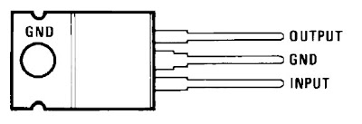
The LM340A monolithic 3-terminal positive voltage regulators employ internal current-limiting, thermal shutdown and safe-area compensation, making them essentially indestructible. If adequate heat sinking is provided, they can deliver over 1.0A output current.

IC LM340A Sesor Suhu
Parameters IC LM340A
  • Output Current: 1000 mA
  • Output Voltage: 7.5, 12, 15, 8, 5 Volt
  • Input Min Voltage: 7.5, 14.8, 10.5, 17.9 Volt
  • Input Max Voltage: 35 Volt
  • Temperature Min: 0 deg C
  • Temperature Max: 70, 125 deg C
  • RegType: Linear Regulator


IC CA3161E Description

The CA3161E is a monolithic integrated circuit that performs the BCD to seven segment decoding function and features constant current segment drivers. When used with the CA3162E A/D Converter the CA3161E provides a complete digital readout system with a minimum number of external parts.

IC CA3161E
Absolute Maximum Ratings IC CA3161E
  • DC VSUPPLY (Between Terminals 1 and 10) . . . . . . . . . . . . . .+7.0V
  • Input Voltage (Terminals 1, 2, 6, 7). . . . . . . . . . . . . . . . . . . . . .+5.5V
  • Output Voltage
  • Output “Off”. . . . . . . . . . . . . . . . . . . . . . . . . . . . . . . . . . . . . . . +7V
  • Output “On” (Note 1) . . . . . . . . . . . . . . . . . . . . . . . . . . . . . . . +10V


IC CA3162E Description

The CA3162E are I2L monolithic A/D converters that provide a 3 digit multiplexed BCD output. They are used with the CA3161E BCD-to-Seven-Segment Decoder/Driver and a minimum of external parts to implement a complete 3-digit display. The CA3162AE is identical to the CA3162E except for an extended operating temperature range.
IC  CA3162E
Absolute Maximum Ratings IC CA3162E
  • DC Supply Voltage (Between Pins 7 and 14) . . . . . . . . . . . . . +7V
  • Input Voltage (Pin 10 or 11 to Ground). . . . . . . . . . . . . . . . . . . 15V
  • Temperature Range CA3162E. . . . . . . . . . . . . . . . . . . . . . . . . . .0 to 75oC
  • Temperature Range CA3162AE . .. . . . . . . . . . . . . . . . . . . . . . -40oC to 85oC
  • Maximum Junction Temperature . . . . . . . . . . . . . . . . . . . . . . . 150oC
  • Maximum Storage Temperature Range . . . . . .. . . . . . . . . . . . .-65oC to 150oC
  • Maximum Lead Temperature (Soldering 10s) . . . . . . . . . . . . . 300oC.
.

READMORE...

Friday, October 09, 2009

Rangkaian Crossover Pasif

Crossover is a tool to limit the "frequency range" to be accepted by the speaker. Imagine the crossover act as police at a traffic, which regulates the flow to the tweeter, the midrange and bass to the subwoofer.


Imagine if there was no crossover, the frequency will be chaos, there is a low frequency stray in tweeter, high frekwesni stray into the subwoofer, so it is not effective and also if there are strange treble sounds in the bass , and also can be broken tweeter for bass voice. so need to let it all directional crossover.

Rangkaian  Crossover Pasif Skema rangkaian crossover pasif


Notes:
  • Capacitor must be non-polar capacitor types with a voltage rating of 50 volt or more (preferably 100 volt).
  • Capacitor may be paralled to achieve specified values.
  • Resistors should be 100 Watts or more.

Cara menentukan nilai induktor

This is the formula to calculate the inductance value of an inductor. Of course, this formula can be inverted to calculate the number of inductor winding inductance if its value is determined.

menentukan Nilai induktor
  • L: inductance in H (Henry)
  • m: permeability core (core), m = 1 (Special inductor without core / winding water)
  • mo: vacuum air permeability, mo = 4p x 10-7
  • N: number of inductor winding
  • A: inductors sectional area (m2)
  • l: length of the inductor (m)

READMORE...

Rangkaian Pengukur kecepatan Udaran

This is a simple wind meter (anemometer) circuit. this circuit can measure wind speeds up to 75m/s using this circuit.

Transistors Q1 and Q2 are used for sensing the wind. The relationship between thermal impedance of the transistor and the surrounding wind speed is utilized here. Transistors Q1 and Q2 are wired so that the Vce of Q1 is higher than Q2 and therefore there will be a higher power dissipation. The wind causes cooling and so the Vce of Q1 changes. The ends in different power dissipations and different voltages across R10. This variation is detected by the opamp and amplified to produce the Vout which is proportional to the wind speed. For still air Vout will be 0V and at 75m/s wind speed the Vout will be 2.5V. A 3V FSD voltmeter connected across the Vout terminal and ground can be used as the display.


For proper working, the air must pass over both the transistors (Q1 and Q2).
The resistors used are not standard values. So you need to use the combination (series or parallel) of resistors to attain the specified values. Please note that the resistor values are very critical in this circuit.


IC LT1013 Description


Absolute maximum ratings IC LT1013
  • Supply voltage : . . . . . . . . . . . . . . . . . .. . . . . . . . . . . . . .. . +22 V/ –22 V
  • Input voltage range, VI (any input) . . . . . . . . . . . . . . . . . . .. . . VCC– –5 V to VCC+
  • Differential input voltage . . . . . . . . . . . . . . . . . . . . . . . . . .. . . 30 V
  • Duration of short-circuit current at (or below) 25 C . . . . . . . . . . Unlimited
  • Package thermal impedance, θJA : D package . . . . . . . . . . . . 97 C/W
  • P package . . . . . . . . . . . . . . . . . . . . . . . . . . . . .. . . . . . . . . 85 C/W
  • Case temperature for 60 seconds: FK package . . . . . . . . . . . . 260 C
  • Lead temperature 1,6 mm (1/16 inch) from case for 10 seconds: D or P package . . . . 260 C
  • JG package . . . . . . . . . . . . . . . . . . . . . . . . . . . . . . . . . . . . . 300 C
  • Storage temperature range, Tstg . . . . . . . . . . . . . . . . . . . .. . . –65 C to 150 C

READMORE...

Rangkaian Remote Control Ultrasonic

This is a remote control circuit employing ultrasonic signals. The ultrasonic transmitter circuit is build around IC1(NE 555). IC1 is an astable multi vibrator operating at 40KHz.The output of IC1 is amplifier the complementary pair of transistors ( Q1 & Q2) and transmitted by the ultrasonic transmitter K1. The switch S1 is used activate the transmitter.

remote ultrasonicSkema rangkaian remote Control ultrasonic


Note:
  • switch S1 can be a push button switch.
  • The preset R16 can be used to adjust the sensitivity of the receiver.
  • The frequency of the ultrasonic signal can be varied by adjusting the preset R17.Adjust it for optimum performance.


The ultrasonic receiver uses an sensor transducer (K2) to sense the ultrasonic signals. When an ultrasonic signal is falling on the sensor, it produces a proportional voltage signal at its output. This weak signal is amplified by the two stage amplifier circuit comprising of transistors Q3 and Q4.The output of the amplifier is rectified by the diodes D3 & D4.The rectified signal is given to the inverting input of the opamp which is wired as a comparator. When ever there is an ultrasonic signal falling on the receiver, the output of the comparator activates the transistors Q5 & Q6 to drive the relay. In this way the load connected via the relay can be switched. The diode D5 is used as a free wheeling diode.


Features IC CA3140


  • Very High Input Impedance (ZIN) -1.5TΩ (Typ)
  • Very Low Input Current (Il) -10pA (Typ) at ±15V
  • Wide Common Mode Input Voltage Range (VlCR) - Can be wung 0.5V Below Negative Supply Voltage Rail
  • Output Swing Complements Input Common Mode
  • Directly Replaces Industry Type 741 in Most Applications
  • Pb-Free Plus Anneal Available (RoHS Compliant)


Pin Connection Ic NE 555


  • Ground, is the input pin of the source of the negative DC voltage
  • Trigger, negative input from the lower comparators (comparator B) that maintain oscillation capacitor voltage in the lowest 1 / 3 Vcc and set RS flip-flop
  • Output, the output pin of the IC 555.
  • Reset, the pin that serves to reset the latch inside the IC to be influential to reset the IC work. This pin is connected to a PNP-type transistor gate, so the transistor will be active if given a logic low. Normally this pin is connected directly to Vcc to prevent reset
  • Control voltage, this pin serves to regulate the stability of the reference voltage negative input (comparator A). This pin can be left hanging, but to ensure the stability of the reference comparator A, usually associated with a capacitor of about 10nF to berorde pin groun
  • Threshold, this pin is connected to the positive input (comparator A) which will reset the RS flip-flop when the voltage on the capacitor from exceeding 2 / 3 Vc
  • Discharge, this pin is connected to an open collector transistor Q1 is connected to ground emitternya. Switching transistor serves to clamp the corresponding node to ground on the timing of certain
  • Vcc, pin it to receive a DC voltage supply. Usually will work optimally if given a 5-15V. the current supply can be seen in the datasheet, which is about 10-15mA.
.

READMORE...

Wednesday, October 07, 2009

Rangkaian Comparator Tegangan

This is a Voltage Comparator circuit can be uses indicates the input voltage differs from two defined limits, V1 and V2.

One application here is to monitor a 12V car battery. V1 can be set to 14V and V2 to 11V thus giving an indication of more than the cost or weak batteries. Op-amp used here is the CA3140 MOSFET. They are used to advantage because they have less output offset voltage and can switch to 0volts close. If any other use op-amps like the LF351 or CA741 will need to have an offset null control. This is just a 10k preset reached between pins 1 and 5, the wiper connected to the negative supply op-amps or 4 pins. The following is a schematic drawing:

Comparator TeganganRangkaian Comparator Tegangan Sederhana

With this circuit the op-amp will turn on the LED if the input voltage out of limits, the two 1N4148 diodes to form an “AND”-gate at the output. Input voltage to be monitored are fed through a series of 10k resistors on the input of both op-amps. If the input voltage is greater than the limit set by V1 it will CA3140 output swing to almost full supply voltage and LED lights. Similarly, if the input voltage is less than the limit set by V2 the op-amp will swing to the Vcc and the LED light.

IC CA3140 Description

The CA3140 is integrated circuit operational amplifiers that combine the advantages of high voltage PMOS transistors with high voltage bipolar transistors on a single monolithic chip.


Absolute Maximum Ratings

DC Supply Voltage (Between V+ and V- Terminals) . . . . . . . . . 36V
Differential Mode Input Voltage . . . . . . . . . . . . . . . . . . . . . . . . . . 8V
DC Input Voltage . . . . . . . . . . . . . . . . . . . . . (V+ +8V) To (V- -0.5V)
Input Terminal Current. . . . . . . . . . . . . . . . . . . . . . . . . . . . . . . . 1mA
Output Short Circuit Duration∞ (Note 2) . . . . . . . . . . . . . . Indefinite
Temperature Range. . . . . . . . . . . . . . . . . . . . . . . . . -55oC to 125oC
Maximum Junction Temperature (Plastic Package) . . . . . . . 150oC
Maximum Storage Temperature Range . . . . . . . . . -65oC to 150oC
Maximum Lead Temperature (Soldering 10s) . . . . . . . . . . . . 300oC

READMORE...

Tuesday, October 06, 2009

Rangkaian Sound Level Meter

This is circuit can be used to check the sound levels.The sound pressure meter is vey useful in setting up home theater systems , if you need to test the sound pressure of each channels on different positions in the room.

The circuit is nothing but a non- inverting amplifier based on op-amp CA 3140. The sound picked by the condenser mic will be amplified by the IC1 and rectified by the bridge D1 to drive the meter M1. The deflection on the meter will be proportional to the pressure of the sound falling on the mic.The switch S1 can be used as an ON/OFF switch.

sound level meterSkema rangkaian sound level meter

Note:
  • The bridge D1 can be a 1A bridge.If 1A bridge is note available,make one using four 1N4007 diodes.
  • The circuit ca be powered by using a 9V PP3 battery.

Pin IC CA3140

The IC CA3140 is integrated circuit operational amplifiers that combine the advantages of high voltage PMOS transistors with high voltage bipolar transistors on a single monolithic chip.

IC CA3140
Features
  • Very High Input Impedance (ZIN) -1.5TΩ (Typ)
  • Very Low Input Current (Il) -10pA (Typ) at ±15V
  • Wide Common Mode Input Voltage Range (VlCR) - Can be Swung 0.5V Below Negative Supply Voltage Rail
  • Output Swing Complements Input Common Mode Range
  • Directly Replaces Industry Type 741 in Most Applications
  • Pb-Free Plus Anneal Available (RoHS Compliant).

READMORE...

Rangkaian Pendeteksi Sinyal Electromagnetic

This is the circuit of electromagnetic field sensor which can sense electromagnetic field from 40Hz to 140Hz. The IC LF351 and associated components forms the pick-up section. 1uH coil L1 is used for sensing the field and the IC1 performs the necessary amplification. If the picked electromagnetic field is in the audio frequency range, it can be heard through the head phone Z1. There is also a meter arrangement for accurate measuring of the signal strength. Transistor Q1 performs additional amplification on the picked signal in order to drive the meter.

 Pendeteksi Sinyal Electromagnetic

Skema Rangkaian Pendeteksi Sinyal Electromagnetic


IC LF351 Description

The IC LF351 is a low cost high speed JFET input operational amplifier with an internally trimmed input offset voltage (BI-FET II™ technology). The device requires a low supply current and yet maintains a large gain bandwidth product and a fast slew rate. In addition, well matched high voltage JFET input devices provide very low input bias and offset currents. The LF351 is pin compatible with the standard LM741 and uses the same offset voltage adjustment circuitry. This feature allows designers to immediately upgrade the overall performance of existing LM741 designs.

The IC LF351 may be used in applications such as high speed integrators, fast D/A converters, sample-and-hold circuits and many other circuits requiring low input offset voltage, low input bias current, high input impedance, high slew rate and wide bandwidth.


Features IC LF351

• Internally trimmed offset voltage: 10 mV
• Low input bias current: 50 pA
• Low input noise voltage: 25 nV/
• Low input noise current: 0.01 pA/
• Wide gain bandwidth: 4 MHz
• High slew rate: 13 V/µs
• Low supply current: 1.8 mA
• High input impedance: 1012 Ohm
• Low total harmonic distortion AV=10,: <0.02% RL=10k, VO=20 Vp-p, BW=20 Hz-20 kHz
• Low 1/f noise corner: 50 Hz
• Fast settling time to 0.01%: 2 µs.
.

READMORE...

Monday, October 05, 2009

Hifi stereo pre-amp head

This is hifi stereo pre-amp head with tone control circuit Using a special IC TDA1524A
All signal processing is done within the TDA1524A by voltage controlled amplifiers and voltage controlled filters. The IC provides a fixed voltage (~ 3.8V DC) at pin 17, and this is used by all the variable resistors to provide an adjustable DC voltage to the appropriate control pins.

Current sensing is used to provide a flat response when R5 is connected to pin 17, and a loudness contour when disconnected. 100 nF capacitors are used on each pot to decouple any AC signals from the control inputs. 10 uF capacitors are used to couple both input and output audio signals whilst blocking DC. R1 and R2, are to ensure stability with capacitive loads. R3 and R4 make sure there are no DC spikes at the output sockets if the load is switched. C3 and C4 control the loudness contour. C5 and C6 control the treble turn-over frequency. C18 and C19 have been added to roll off the gain above 70 kHz. Low volume settings coupled with treble boost was causing HF instability in some instances. This should no longer be a problem.

Hifi stereo pre-amp headSkema rangkaian hifi stereo pre-amp head


C15, 16, 17 provide power supply filtering. D1 provides protection in case of incorrect supply polarity. The LED is a power on indicator and may be omitted if not required, or preferably mounted on the enclosure. If you are not using a switch pot, you can connect an external switch across the P1 switch pins, or connect a wire link there and switch the power supply.

The power supply is critical to the noise performance of the pre-amp head. An on board regulator is provided to reduce mains hum. If you wish to use it with a car or other 12V battery, then you should omit the 7812 regulator, and place a wire link between the regulator input and output pin positions on the PC board. Do not short to earth! This will be necessary because the regulator must have an input voltage at least 2-3V greater than it’s output, for it to maintain regulation. However the regulator will not be necessary with a battery supply.

If using a plug pack, it’s output voltage should be 15 to 18V DC. Because most plug packs have poor regulation, one rated at 12V DC will often be around 15V when lightly loaded. The current drain of the pre-amp is less than 50 mA, so many 12 V unregulated supplies may be adequate if you have one. Replace D1 with a wire link if necessary, making sure you have the supply polarity correct!

If you are using a 15-20V supply for your power amplifier, you can use that as your pre-amp supply as well. Make sure you test the voltage first in all cases.

READMORE...

Saturday, October 03, 2009

Rangkaian Saklar Sentuh

This is a Turn on and turn off your electrical devices using touch switch, so you can “play” your electronic devices more fun. Touch switch don’t need mechanical part, so they will not worn out due to mechanical contact. Touch switches can be used in places where regular switches would not last, such as wet or very dusty areas. You just need to add some relay to switch your devices which require high voltage supply.


saklar sentuh
Skema rangkaian saklar sentuh


Component list:

C1: 10uF/16V Electrolytic Capacitor
R1, R2: 100K 1/4 Watt Resistor
R3: 10 Meg 1/4 Watt Resistor
U1: 4011 CMOS NAND Gate IC
MISC 1 Board, Wire, Socket For U1


Notes:
  • The contacts an be made with just two loops of wire close together, or two squares etched close together on a PC board.
  • When activated, the output of the circuit goes high for about one second. This pulse can be used to drive a relay, transistor, other logic, etc.
  • You can vary the length of the output pulse by using a smaller or larger capacitor for C1.


IC 4011 Description:

The HEF4011B provides the positive quadruple 2-input NAND function. The HEF4011 have equal source and sink current capabilities and conform to standard B series output drive.
The devices also have buffered outputs which improve transfer characteristics by providing very high gain. All inputs are protected against static discharge with diodes to VDD and VSS.


The HEF4011B Features

Low power TTL: Fan out of 2 driving 74L compatibility: or 1 driving 74LS
5V–10V–15V parametric ratings
Symmetrical output characteristics
Maximum input leakage 1 μA at 15V over full
temperature range.
.

READMORE...
 
Skema Rangkaian Elektronika